参数资料
| 型号: | ICL7612BCPAZ |
| 厂商: | Intersil |
| 文件页数: | 10/13页 |
| 文件大小: | 0K |
| 描述: | IC OPAMP LOW PWR 1.4MHZ 8-DIP |
| 标准包装: | 50 |
| 放大器类型: | 通用 |
| 电路数: | 1 |
| 转换速率: | 1.6 V/µs |
| 增益带宽积: | 1.4MHz |
| 电流 - 输入偏压: | 1pA |
| 电压 - 输入偏移: | 5000µV |
| 电流 - 电源: | 1mA |
| 电流 - 输出 / 通道: | 40mA |
| 电压 - 电源,单路/双路(±): | 2 V ~ 16 V,±1 V ~ 8 V |
| 工作温度: | 0°C ~ 70°C |
| 安装类型: | 通孔 |
| 封装/外壳: | 8-DIP(0.300",7.62mm) |
| 供应商设备封装: | 8-PDIP |
| 包装: | 管件 |
6
FN2919.9
April 26, 2007
Application Information
Static Protection
All devices are static protected by the use of input diodes.
However, strong static fields should be avoided, as it is
possible for the strong fields to cause degraded diode
junction characteristics, which may result in increased input
leakage currents.
Latchup Avoidance
Junction-isolated CMOS circuits employ configurations which
produce a parasitic 4-layer (PNPN) structure. The 4-layer
structure has characteristics similar to an SCR, and under
certain circumstances may be triggered into a low impedance
state resulting in excessive supply current. To avoid this
condition, no voltage greater than 0.3V beyond the supply
rails may be applied to any pin. In general, the op amp
supplies must be established simultaneously with, or before
any input signals are applied. If this is not possible, the drive
circuits must limit input current flow to 2mA to prevent latchup.
Choosing the Proper IQ
The ICL7611 and ICL7612 have a similar IQ set-up scheme,
which allows the amplifier to be set to nominal quiescent
currents of 10
μA, 100μA or 1mA. These current settings
change only very slightly over the entire supply voltage
range. The ICL7611 and ICL7612 have an external IQ
control terminal, permitting user selection of quiescent
current. To set the IQ connect the IQ terminal as follows:
IQ = 10μA - IQ pin to V+
IQ = 100μA - IQ pin to ground. If this is not possible, any
voltage from V+ - 0.8 to V- +0.8 can be used.
IQ = 1mA - IQ pin to V-
NOTE: The output current available is a function of the quiescent
current setting. For maximum peak-to-peak output voltage swings
into low impedance loads, IQ of 1mA should be selected.
Output Stage and Load Driving Considerations
Each amplifiers’ quiescent current flows primarily in the
output stage. This is approximately 70% of the IQ settings.
This allows output swings to almost the supply rails for
output loads of 1M
Ω, 100kΩ, and 10kΩ, using the output
stage in a highly linear class A mode. In this mode,
crossover distortion is avoided and the voltage gain is
maximized. However, the output stage can also be operated
in Class AB for higher output currents. (See graphs under
Typical Operating Characteristics). During the transition from
Class A to Class B operation, the output transfer
characteristic is non-linear and the voltage gain decreases.
Input Offset Nulling
Offset nulling may be achieved by connecting a 25k pot
between the BAL terminals with the wiper connected to V+.
At quiescent currents of 1mA and 100
μA the nulling range
provided is adequate for all VOS selections; however with
IQ =10μA, nulling may not be possible with higher values
of VOS.
Frequency Compensation
The ICL7611 and ICL7612 are internally compensated, and
are stable for closed loop gains as low as unity with
capacitive loads up to 100pF.
Extended Common Mode Input Range
The ICL7612 incorporates additional processing which
allows the input CMVR to exceed each power supply rail by
0.1V for applications where VSUPP ≥ ±1.5V. For those
applications where VSUPP ≤ ±1.5V the input CMVR is limited
in the positive direction, but may exceed the negative supply
rail by 0.1V in the negative direction (e.g., for VSUPPLY = ±1V,
the input CMVR would be +0.6V to -1.1V).
Operation At VSUPPLY = ±1V
Operation at VSUPPLY = ±1V is guaranteed at IQ = 10μA for
A and B grades only.
Output swings to within a few millivolts of the supply rails are
achievable for RL ≥ 1MΩ. Guaranteed input CMVR is ±0.6V
minimum and typically +0.9V to -0.7V at VSUPPLY = ±1V. For
applications where greater common mode range is
desirable, refer to the description of ICL7612 above.
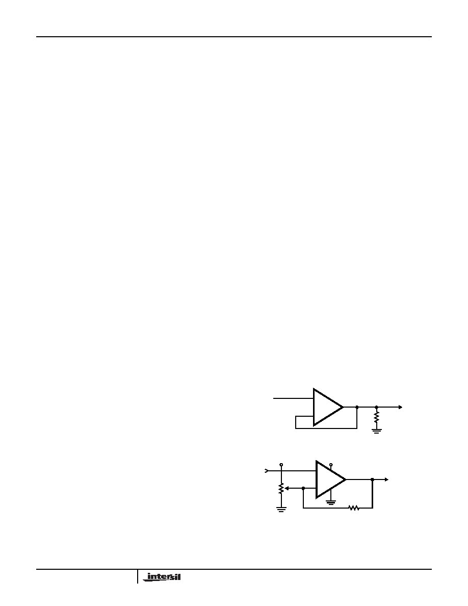
Typical Applications
The user is cautioned that, due to extremely high input
impedances, care must be exercised in layout, construction,
board cleanliness, and supply filtering to avoid hum and
noise pickup.
Note that in no case is IQ shown. The value of IQ must be
chosen by the designer with regard to frequency response
and power dissipation.
ICL7612
+
-
VIN
VOUT
RL ≥10k
FIGURE 1. SIMPLE FOLLOWER (NOTE 4)
ICL7612
+
-
VIN
VOUT
100k
+5
1M
TO CMOS OR
LPTTL LOGIC
NOTE:
4. By using the ICL7612 in this application, the circuit will follow rail
to rail inputs.
FIGURE 2. LEVEL DETECTOR (NOTE 4)
ICL7611, ICL7612
相关PDF资料 |
PDF描述 |
|---|---|
| ICL7614ACPA+ | IC OPAMP LP CMOS 8-DIP |
| ICL7621DCBAZ | IC OPAMP DUAL 0.5MHZ CMOS 8-SOIC |
| ICL7650CSD+T | IC OPAMP CHOPPER/STABLE 14-SOIC |
| ICL7650SCBA-1ZT | IC OPAMP 2MHZ CHOPPER STBL 8SOIC |
| ICL7652CWE+T | IC OPAMP CHOPPER/STABLE 16-SOIC |
相关代理商/技术参数 |
参数描述 |
|---|---|
| ICL7612BCPD | 制造商:MAXIM 制造商全称:Maxim Integrated Products 功能描述:Single/Dual/Triple/Quad Operational Amplifiers |
| ICL7612BCPE | 制造商:MAXIM 制造商全称:Maxim Integrated Products 功能描述:Single/Dual/Triple/Quad Operational Amplifiers |
| ICL7612BCSA | 功能描述:运算放大器 - 运放 Single CMOS Low Power RoHS:否 制造商:STMicroelectronics 通道数量:4 共模抑制比(最小值):63 dB 输入补偿电压:1 mV 输入偏流(最大值):10 pA 工作电源电压:2.7 V to 5.5 V 安装风格:SMD/SMT 封装 / 箱体:QFN-16 转换速度:0.89 V/us 关闭:No 输出电流:55 mA 最大工作温度:+ 125 C 封装:Reel |
| ICL7612BCSA+ | 功能描述:运算放大器 - 运放 Single CMOS Low Power RoHS:否 制造商:STMicroelectronics 通道数量:4 共模抑制比(最小值):63 dB 输入补偿电压:1 mV 输入偏流(最大值):10 pA 工作电源电压:2.7 V to 5.5 V 安装风格:SMD/SMT 封装 / 箱体:QFN-16 转换速度:0.89 V/us 关闭:No 输出电流:55 mA 最大工作温度:+ 125 C 封装:Reel |
| ICL7612BCSA+T | 功能描述:运算放大器 - 运放 Single CMOS Low Power RoHS:否 制造商:STMicroelectronics 通道数量:4 共模抑制比(最小值):63 dB 输入补偿电压:1 mV 输入偏流(最大值):10 pA 工作电源电压:2.7 V to 5.5 V 安装风格:SMD/SMT 封装 / 箱体:QFN-16 转换速度:0.89 V/us 关闭:No 输出电流:55 mA 最大工作温度:+ 125 C 封装:Reel |
发布紧急采购,3分钟左右您将得到回复。