参数资料
| 型号: | ICL7650SCBA-1T |
| 厂商: | Intersil |
| 文件页数: | 8/13页 |
| 文件大小: | 0K |
| 描述: | IC OPAMP 2MHZ CHOPPER STBL 8SOIC |
| 标准包装: | 2,500 |
| 放大器类型: | 断路器(零漂移) |
| 电路数: | 1 |
| 转换速率: | 2.5 V/µs |
| 增益带宽积: | 2MHz |
| 电流 - 输入偏压: | 4pA |
| 电压 - 输入偏移: | 700µV |
| 电流 - 电源: | 2mA |
| 电流 - 输出 / 通道: | 30mA |
| 电压 - 电源,单路/双路(±): | 4.5 V ~ 16 V,±2.25 V ~ 8 V |
| 工作温度: | 0°C ~ 70°C |
| 安装类型: | 表面贴装 |
| 封装/外壳: | 8-SOIC(0.154",3.90mm 宽) |
| 供应商设备封装: | 8-SOIC |
| 包装: | 带卷 (TR) |
4
FN2920.10
April 12, 2007
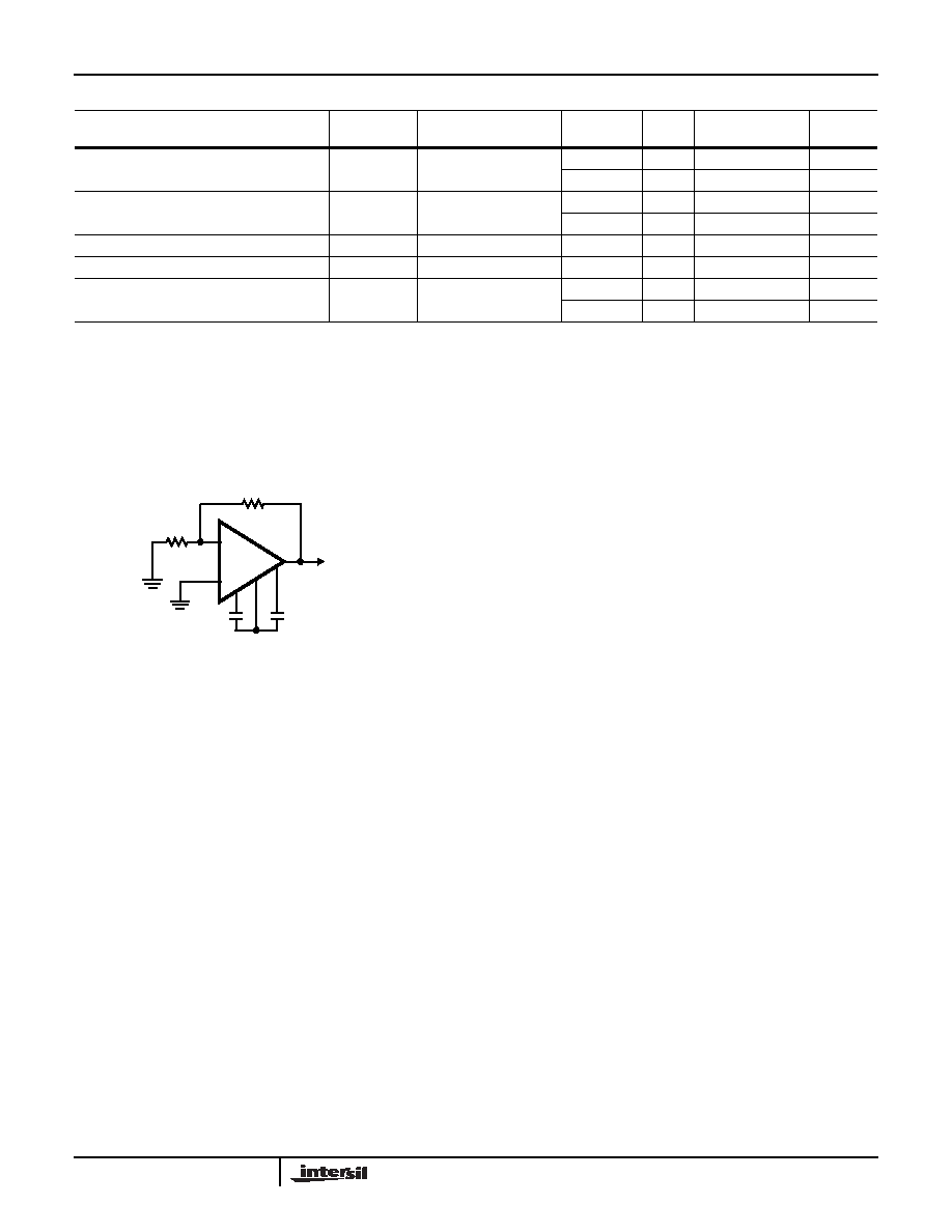
Test Circuit
Application Information
Detailed Description
AMPLIFIER
The functional diagram shows the major elements of the
ICL7650S. There are two amplifiers, the main amplifier, and the
nulling amplifier. Both have offset-null capability. The main
amplifier is connected continuously from the input to the output,
while the nulling amplifier, under the control of the chopping
oscillator and clock circuit, alternately nulls itself and the main
amplifier. The nulling connections, which are MOSFET gates,
are inherently high impedance, and two external capacitors
provide the required storage of the nulling potentials and the
necessary nulling-loop time constants. The nulling arrangement
operates over the full common-mode and power-supply
ranges, and is also independent of the output level, thus giving
exceptionally high CMRR, PSRR, and AVOL.
Careful balancing of the input switches, and the inherent
balance of the input circuit, minimizes chopper frequency
charge injection at the input terminals, and also the feed
forward-type injection into the compensation capacitor, which
is the main cause of output spikes in this type of circuit.
INTERMODULATION
Previous chopper-stabilized amplifiers have suffered from
intermodulation effects between the chopper frequency and
input signals. These arise because the finite AC gain of the
amplifier necessitates a small AC signal at the input. This is
seen by the zeroing circuit as an error signal, which is
chopped and fed back, thus injecting sum and difference
frequencies and causing disturbances to the gain and phase
vs frequency characteristics near the chopping frequency.
These effects are substantially reduced in the ICL7650S by
feeding the nulling circuit with a dynamic current,
corresponding to the compensation capacitor current, in such
a way as to cancel that portion of the input signal due to finite
AC gain. Since that is the major error contribution to the
ICL7650S, the intermodulation and gain/phase disturbances
are held to very low values, and can generally be ignored.
CAPACITOR CONNECTION
The null/storage capacitors should be connected to the
CEXTA and CEXTB pins, with a common connection to the
CRETN pin. This connection should be made directly by
either a separate wire or PC trace to avoid injecting load
current IR drops into the capacitive circuitry. The outside foil,
where available, should be connected to CRETN.
OUTPUT CLAMP
The OUTPUT CLAMP pin allows reduction of the overload
recovery time inherent with chopper-stabilized amplifiers.
When tied to the inverting input pin, or summing junction, a
current path between this point and the OUTPUT pin occurs
just before the device output saturates. Thus uncontrolled
input differentials are avoided, together with the consequent
charge buildup on the correction-storage capacitors. The
output swing is slightly reduced.
Output Source Current
IO SOURCE
+25
2.9
4.5
-
mA
0 to +70
2.3
-
mA
Output Sink Current
IO SINK
+2525
30-
mA
0 to +70
20
-
mA
Internal Chopping Frequency
fCH
Pins 13 and 14 Open
+25
120
250
375
Hz
Clamp ON Current (Note 5)
RL = 100kΩ
+2525
70-
μA
Clamp OFF Current (Note 5)
-4V
≤ VOUT ≤ +4V
+25
-
0.001
5
nA
0 to +70
-
10
nA
NOTES:
3. These parameters are guaranteed by design and characterization, but not tested at temperature extremes because thermocouple effects prevent
precise measurement of these voltages in automatic test equipment.
4. OUTPUT CLAMP not connected. See typical characteristic curves for output swing vs clamp current characteristics.
5. See OUTPUT CLAMP under detailed description.
6. All significant improvements over the industry-standard ICL7650 are highlighted in bold italics.
Electrical Specifications
VSUPPLY = ±5V. See Test Circuit, Unless Otherwise Specified (Continued)
PARAMETER
SYMBOL
TEST CONDITIONS
TEMP.
(°C)
MIN
TYP
MAX
UNITS
ICL7650S
+
-
OUTPUT
R2
1M
Ω
C
CR
0.1
μF0.1μF
C
R1
1M
Ω
相关PDF资料 |
PDF描述 |
|---|---|
| TA45-A326M150C0 | CIRCUIT BRKR THERMAL 15A 2POLE |
| ICL7650SCBA-1 | IC OPAMP 2MHZ CHOPPER STBL 8SOIC |
| AD8132AR-REEL7 | IC AMP DIFF LDIST LP 70MA 8SOIC |
| TA45-A324LJ04C0 | CIRC BREAKER ROCKER 2 POLE |
| ICL7621DCPA | IC OPAMP DUAL 0.5MHZ CMOS 8-DIP |
相关代理商/技术参数 |
参数描述 |
|---|---|
| ICL7650SCBA-1Z | 功能描述:运算放大器 - 运放 OPAMP SUPER CHOPPER STABILIZED COM RoHS:否 制造商:STMicroelectronics 通道数量:4 共模抑制比(最小值):63 dB 输入补偿电压:1 mV 输入偏流(最大值):10 pA 工作电源电压:2.7 V to 5.5 V 安装风格:SMD/SMT 封装 / 箱体:QFN-16 转换速度:0.89 V/us 关闭:No 输出电流:55 mA 最大工作温度:+ 125 C 封装:Reel |
| ICL7650SCBA-1ZT | 功能描述:运算放大器 - 运放 OPAMP SUPER CHOPPER STABILIZED COMEL RoHS:否 制造商:STMicroelectronics 通道数量:4 共模抑制比(最小值):63 dB 输入补偿电压:1 mV 输入偏流(最大值):10 pA 工作电源电压:2.7 V to 5.5 V 安装风格:SMD/SMT 封装 / 箱体:QFN-16 转换速度:0.89 V/us 关闭:No 输出电流:55 mA 最大工作温度:+ 125 C 封装:Reel |
| ICL7650SCBD | 制造商:Rochester Electronics LLC 功能描述:- Bulk |
| ICL7650SCPA-1 | 功能描述:IC OPAMP CHOP/STABALZR 2MHZ 8DIP RoHS:否 类别:集成电路 (IC) >> Linear - Amplifiers - Instrumentation 系列:- 标准包装:1,000 系列:- 放大器类型:电压反馈 电路数:4 输出类型:满摆幅 转换速率:33 V/µs 增益带宽积:20MHz -3db带宽:30MHz 电流 - 输入偏压:2nA 电压 - 输入偏移:3000µV 电流 - 电源:2.5mA 电流 - 输出 / 通道:30mA 电压 - 电源,单路/双路(±):4.5 V ~ 16.5 V,±2.25 V ~ 8.25 V 工作温度:-40°C ~ 85°C 安装类型:表面贴装 封装/外壳:14-SOIC(0.154",3.90mm 宽) 供应商设备封装:14-SOIC 包装:带卷 (TR) |
| ICL7650SCPA-1R2207 | 制造商:Rochester Electronics LLC 功能描述:- Bulk |
发布紧急采购,3分钟左右您将得到回复。