参数资料
| 型号: | ICL7665SIBA |
| 厂商: | Intersil |
| 文件页数: | 7/14页 |
| 文件大小: | 0K |
| 描述: | IC VOLT DETECTOR OVER/UND 8-SOIC |
| 标准包装: | 98 |
| 类型: | 多压监控器 |
| 监视电压数目: | 2 |
| 输出: | 开路漏极或开路集电极 |
| 复位: | 高有效 |
| 电压 - 阀值: | 可调节/可选择 |
| 工作温度: | -40°C ~ 85°C |
| 安装类型: | 表面贴装 |
| 封装/外壳: | 8-SOIC(0.154",3.90mm 宽) |
| 供应商设备封装: | 8-SOIC |
| 包装: | 管件 |
�� �
�
�ICL7665S�
�Detailed� Description�
�As� shown� in� the� Functional� Diagram,� the� ICL7665S� consists�
�of� two� comparators� which� compare� input� voltages� on� the�
�SET1� and� SET2� terminals� to� an� internal� 1.3V� bandgap�
�reference.� The� outputs� from� the� two� comparators� drive�
�open-drain� N-channel� transistors� for� OUT1� and� OUT2,� and�
�open-drain� P-channel� transistors� for� HYST1� and� HYST2�
�outputs.� Each� section,� the� Undervoltage� Detector� and� the�
�Overvoltage� Detector,� is� independent� of� the� other,� although�
�both� use� the� internal� 1.3V� reference.� The� offset� voltages� of�
�the� two� comparators� will� normally� be� unequal� so� V� SET1� will�
�generally� not� quite� equal� V� SET2� .�
�The� input� impedance� of� the� SET1� and� SET2� pins� are�
�extremely� high,� and� for� most� practical� applications� can� be�
�ignored.� The� four� outputs� are� open-drain� MOS� transistors,�
�and� when� ON� behave� as� low� resistance� switches� to� their�
�If� the� SET� voltages� must� be� applied� before� the� supply� voltage�
�V+,� the� input� current� should� be� limited� to� less� than� 0.5mA� by�
�appropriate� external� resistors,� usually� required� for� voltage�
�setting� anyway.� A� similar� precaution� should� be� taken� with� the�
�outputs� if� it� is� likely� that� they� will� be� driven� by� other� circuits� to�
�levels� outside� the� supplies� at� any� time.�
�Additionally,� with� a� V+� supply� that� has� ringing� or� drooping� after�
�power� up,� a� false� transition� on� the� OUTx� output� may� occur�
�even� though� the� resistor� programmed� threshold� voltage� is� not�
�encroached� upon.� This� occurs� as� the� internal� bandgap� circuit�
�time� constant,� on� the� order� of� a� microsecond� is� matched� by� the�
�V+� transient.� If� this� occurs� connecting� a� 1� μ� F� to� the� SETx� pin� will�
�eliminate� the� OUTx� false� transition� as� the� additional�
�capacitance� moves� the� external� time� constant� three� orders� of�
�magnitude� above� the� internal� time� constant.�
�respective� supply� rails.� This� minimizes� errors� in� setting� up�
�the� hysteresis,� and� maximizes� the� output� flexibility.� The�
�INPUT�
�V� SET1� ,�
�V� SET2�
�1.6V�
�1.0V�
�operating� currents� of� the� bandgap� reference� and� the�
�comparators� are� around� 100nA� each.�
�OUT1�
�t� SO1D�
�t� O1F�
�t� SO1D�
�t� O1R�
�V+�
�(5V)�
�V+�
�GND�
�4.7k� Ω�
�OUT1�
�t� SH1D�
�t� H1R�
�t� H1F�
�V+�
�(5V)�
�INPUT�
�1� OUT1� V+� 8�
�2� HYST1� OUT2� 7�
�3� SET1� SET2� 6�
�4� GND� HYST2� 5�
�4.7�
�k� Ω�
�HYST1�
�OUT2�
�HYST2�
�HYST1�
�OUT2�
�t� SO2D�
�t� O2R�
�t� SH2� D�
�t� H2R�
�t� SH1D�
�t� SO2D�
�t� O2F�
�t� SH2D�
�t� H2F�
�GND�
�V+�
�(5V)�
�GND�
�V+�
�(5V)�
�HYST2�
�GND�
�20�
�k� Ω�
�20�
�k� Ω�
�12�
�pF�
�12�
�pF�
�12�
�pF�
�12�
�pF�
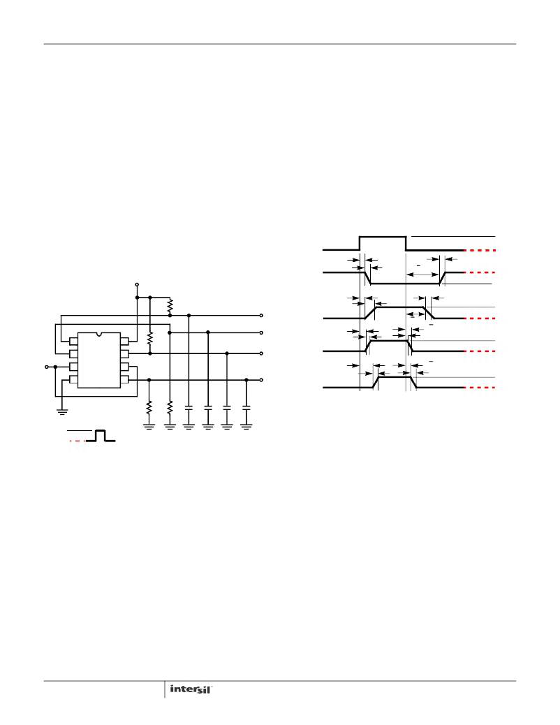
�FIGURE� 8.� SWITCHING� WAVEFORMS�
�V� SET1� =� V� IN� --------------------------------� V� SET2� =� V� IN� --------------------------------�
�(� R� +� R� )� (� R� +� R� )�
�V� TR1� =� V� SET1� ----------------------------------� =� 1.3� ----------------------------------� for� detector� 1�
�R� R�
�V� TR2� =� V� SET2� ----------------------------------� =� 1.3� ----------------------------------� for� detector� 2�
�1.6V�
�1.0V�
�FIGURE� 7.� TEST� CIRCUITS�
�Precautions�
�Junction� isolated� CMOS� devices� like� the� ICL7665S� have� an�
�inherent� SCR� or� 4-layer� PNPN� structure� distributed� throughout�
�the� die.� Under� certain� circumstances,� this� can� be� triggered� into�
�a� potentially� destructive� high� current� mode.� This� latchup� can� be�
�triggered� by� forward-biasing� an� input� or� output� with� respect� to�
�the� power� supply,� or� by� applying� excessive� supply� voltages.� In�
�very� low� current� analog� circuits,� such� as� the� ICL7665S,� this�
�SCR� can� also� be� triggered� by� applying� the� input� power� supply�
�extremely� rapidly� (“instantaneously”),� e.g.,� through� a� low�
�impedance� battery� and� an� ON/OFF� switch� with� short� lead�
�lengths.� The� rate-of-rise� of� the� supply� voltage� can� exceed�
�100V/� μ� s� in� such� a� circuit.� A� low� impedance� capacitor� (e.g.,�
�0.05� μ� F� disc� ceramic)� between� the� V+� and� GND� pins� of� the�
�ICL7665S� can� be� used� to� reduce� the� rate-of-rise� of� the� supply�
�voltage� in� battery� applications.� In� line� operated� systems,� the�
�rate-of-rise� of� the� supply� is� limited� by� other� considerations,� and�
�is� normally� not� a� problem.�
�7�
�Simple� Threshold� Detector�
�Figure� 9� shows� the� simplest� connection� of� the� ICL7665S� for�
�threshold� detection.� From� the� graph� 9B,� it� can� be� seen� that�
�at� low� input� voltage� OUT1� is� OFF,� or� high,� while� OUT2� is�
�ON,� or� low.� As� the� input� rises� (e.g.,� at� power-on)� toward�
�V� NOM� (usually� the� eventual� operating� voltage),� OUT2� goes�
�high� on� reaching� V� TR2� .� If� the� voltage� rises� above� V� NOM� as�
�much� as� V� TR1� ,� OUT1� goes� low.� The� Equations� are� giving�
�V� SET1� and� V� SET2� are� from� Figure� 9A:�
�R� 11� R� 12�
�11� 21� 12� 22�
�Since� the� voltage� to� trip� each� comparator� is� nominally� 1.3V,�
�the� value� V� IN� for� each� trip� point� can� be� found� from�
�(� R� 11� +� R� 21� )� (� R� 11� +� R� 21� )�
�11� 11�
�and�
�(� R� 12� +� R� 22� )� (� R� 12� +� R� 22� )�
�R� 12� R� 12�
�FN3182.9�
�July� 22,� 2013�
�相关PDF资料 |
PDF描述 |
|---|---|
| ICL7673CBA-T | IC SWITCH BATTERY BACKUP 8-SOIC |
| ICL8069DESA | IC VREF SHUNT 1.23V 8-SOIC |
| ICM7211AMIPL | IC LCD DISPLAY DRVR 4DGT 40-DIP |
| ICM7212AMIQH-D | IC DECODR/DVR LED 4DIGIT 44PLCC |
| ICM7218BIJI | IC DRIVER DECODER 8DIG 28-CDIP |
相关代理商/技术参数 |
参数描述 |
|---|---|
| ICL7665SIBA-T | 功能描述:电压监测器/监控器 CMOS OVER/UNDER V DETECTOR IND TAPE & RoHS:否 制造商:Texas Instruments 监测电压数:2 监测电压:Adjustable 输出类型:Open Drain 欠电压阈值: 过电压阈值: 准确性:1 % 工作电源电压:1.5 V to 6.5 V 工作电源电流:1.8 uA 最大工作温度:+ 125 C 封装 / 箱体:SON-6 安装风格:SMD/SMT |
| ICL7665SIBA-TS2576 | 制造商:Rochester Electronics LLC 功能描述:- Bulk |
| ICL7665SIBAZ | 功能描述:电压监测器/监控器 CMOS OVER/UNDER V DETECTOR IND RoHS:否 制造商:Texas Instruments 监测电压数:2 监测电压:Adjustable 输出类型:Open Drain 欠电压阈值: 过电压阈值: 准确性:1 % 工作电源电压:1.5 V to 6.5 V 工作电源电流:1.8 uA 最大工作温度:+ 125 C 封装 / 箱体:SON-6 安装风格:SMD/SMT |
| ICL7665SIBAZA | 功能描述:电压监测器/监控器 W/ANNEAL CMOS OVER/ UNDER V DETECTOR RoHS:否 制造商:Texas Instruments 监测电压数:2 监测电压:Adjustable 输出类型:Open Drain 欠电压阈值: 过电压阈值: 准确性:1 % 工作电源电压:1.5 V to 6.5 V 工作电源电流:1.8 uA 最大工作温度:+ 125 C 封装 / 箱体:SON-6 安装风格:SMD/SMT |
| ICL7665SIBAZA-T | 功能描述:电压监测器/监控器 W/ANNEAL CMOS OVER/ UNDER V DETECTOR RoHS:否 制造商:Texas Instruments 监测电压数:2 监测电压:Adjustable 输出类型:Open Drain 欠电压阈值: 过电压阈值: 准确性:1 % 工作电源电压:1.5 V to 6.5 V 工作电源电流:1.8 uA 最大工作温度:+ 125 C 封装 / 箱体:SON-6 安装风格:SMD/SMT |
发布紧急采购,3分钟左右您将得到回复。