- 您现在的位置:买卖IC网 > PDF目录175707 > ICPL2601-SM (ISOCOM COMPONENTS LTD) 1 CHANNEL LOGIC OUTPUT OPTOCOUPLER, 10 Mbps PDF资料下载
参数资料
| 型号: | ICPL2601-SM |
| 厂商: | ISOCOM COMPONENTS LTD |
| 元件分类: | 光电耦合器 |
| 英文描述: | 1 CHANNEL LOGIC OUTPUT OPTOCOUPLER, 10 Mbps |
| 文件页数: | 3/4页 |
| 文件大小: | 226K |
| 代理商: | ICPL2601-SM |
SWITCHING SPECIFICATIONS AT T
A = 25°C ( VCC = 5V, IF = 7.5mA Unless otherwise noted )
PARAMETER
SYM DEVICE
MIN TYP MAX UNITS TEST CONDITION
Propagation Delay Time
to Logic Low at Output
t
PHL
55
75
ns
R
L = 350, CL = 15pF
( fig 1 )( note4 )
Propagation Delay Time
to Logic High at Output
t
PLH
45
75
ns
R
L = 350, CL = 15pF
( fig 1 )( note5 )
Propagation Delay Time
of Enable from V
EH to VEL
t
EHL
14
ns
R
L = 350, CL = 15pF
( note6 )
V
EL = 0V, VEH = 3V
Propagation Delay Time
of Enable from V
EL to VEH
t
ELH
25
ns
R
L = 350, CL = 15pF
( note7 )
V
EL = 0V, VEH = 3V
Common Mode Transient
Immunity at Logic High
CM
H
6N137
10000
V/
s
I
F = 0mA, VCM = 50VPP
Level Output ( fig 2 )( note8 )
ICPL2601
1000 10000
V/
s
R
L= 350,VOH= 2Vmin.
Common Mode Transient
Immunity at Logic Low
CM
L
6N137
-10000
V/
s
V
CM= 50VPP
Level Output ( fig 2 )( note9 )
ICPL2601 -1000 -10000
V/
s
R
L=350,VOL=0.8Vmax.
NOTES:-
1
Bypassing of the power supply line is required, with a 0.01
F ceramic disc capacitor adjacent to
each isolator. The power supply bus for the isolator(s) should be seperate from the bus for any
active loads. Otherwise a larger value of bypass capacitor (up to 0.1
F) may be needed to supress
regenerative feedback via the power supply.
2
Peaking circuits may produce transient input currents up to 50mA, 50ns maximum pulse width,
provided average current does not exceed 20mA.
3
Device considered a two terminal device; pins 1, 2, 3, and 4 shorted together, and pins 5, 6, 7
and 8 shorted together.
4
The t
PHL
propagation delay is measured from the 3.75 mA level Low to High transition of the input
current pulse to the 1.5V level on the High to Low transition of the output voltage pulse.
5
The t
PLH propagation delay is measured from the 3.75mA level High to Low transition of the input
current pulse to the 1.5V level on the Low to High transition of the output voltage pulse.
6
The t
EHL enable input propagation delay is measured from the 1.5V level on the Low to High transition of
the enable input voltage pulse to the 1.5V level on the High to Low of the output voltage pulse.
7
The t
ELH enable input propagation delay is measured from the 1.5V level on the High to Low transition of
the enable input voltage pulse to the 1.5V level on the Low to High of the output voltage pulse.
8
CM
H is the maximum tolerable rate of rise of the common mode voltage to assure that the output
will remain in a high logic state (ie Vout > 2.0V).
9
CM
L is the maximum tolerable rate of fall of the common mode voltage to assure that the output
will remain in a low logic state (ie Vout < 0.8V)
10
No external pull up is required for a high logic state on the enable input.
DB91063-AAS/A1
19/4/99
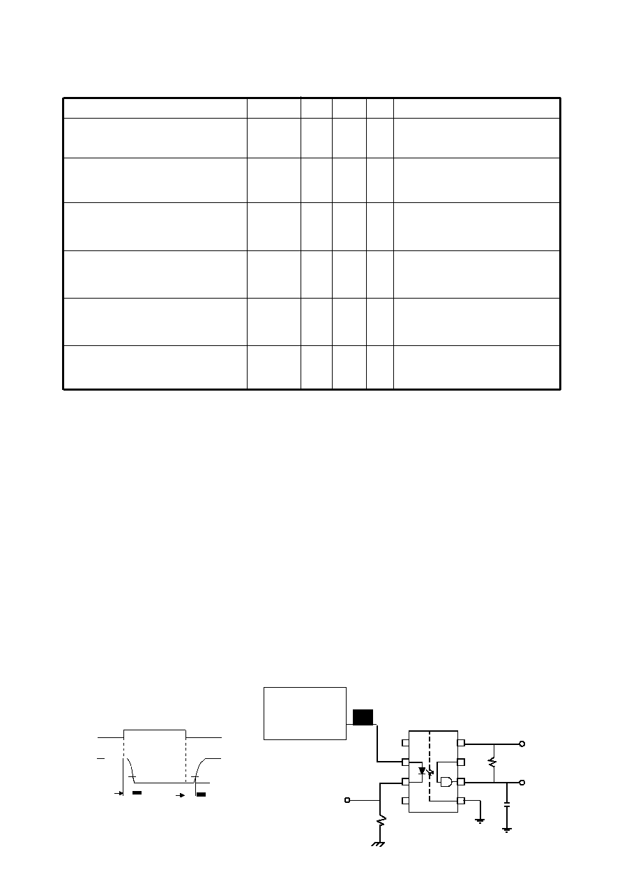
FIG.1 SWITCHING TEST CIRCUIT
2
I
F Monitor
0
I
F
V
O
1.5V
100
1.5V
5V
t
PHL
t
PLH
V
OL
R
L
V
O
C
L = 15pF
8
7
6
5
PULSE
GENERATOR
Z
O = 50
t
r = 5ns
I
F
1
4
3
10% Duty Cycle
1/f < 100
s
5V
相关PDF资料 |
PDF描述 |
|---|---|
| ICS-306-S | DIP6, IC SOCKET |
| ICS2001-LF | SPECIALTY CONSUMER CIRCUIT |
| ICS2001-LF | SPECIALTY CONSUMER CIRCUIT |
| ICS2001 | SPECIALTY CONSUMER CIRCUIT |
| ICS2002V | SPECIALTY CONSUMER CIRCUIT, PQCC44 |
相关代理商/技术参数 |
参数描述 |
|---|---|
| ICPL2611 | 制造商:未知厂家 制造商全称:未知厂家 功能描述:HIGH CMR, VERY HIGH SPEED OPTICALLY COUPLED ISOLATOR LOGIC GATE OUTPUT |
| ICPL2630 | 制造商:未知厂家 制造商全称:未知厂家 功能描述:DUAL CHANNEL, HIGH CMR, VERY HIGH SPEED OPTICALLY COUPLED ISOLATOR LOGIC GATE OUTPUT |
| ICPL2630_12 | 制造商:ISOCOM 制造商全称:ISOCOM 功能描述:DESCRIPTION |
| ICPL2631 | 制造商:未知厂家 制造商全称:未知厂家 功能描述:DUAL CHANNEL, HIGH CMR, VERY HIGH SPEED OPTICALLY COUPLED ISOLATOR LOGIC GATE OUTPUT |
| ICPL2730 | 制造商:未知厂家 制造商全称:未知厂家 功能描述:HIGH SPEED DUAL CHANNEL OPTICALLY COUPLED ISOLATOR PHOTODARLINGTON OUTPUT |
发布紧急采购,3分钟左右您将得到回复。