- 您现在的位置:买卖IC网 > PDF目录65529 > ICS527R-02I (INTEGRATED DEVICE TECHNOLOGY INC) 527 SERIES, PLL BASED CLOCK DRIVER, 2 TRUE OUTPUT(S), 0 INVERTED OUTPUT(S), PDSO28 PDF资料下载
参数资料
| 型号: | ICS527R-02I |
| 厂商: | INTEGRATED DEVICE TECHNOLOGY INC |
| 元件分类: | 时钟及定时 |
| 英文描述: | 527 SERIES, PLL BASED CLOCK DRIVER, 2 TRUE OUTPUT(S), 0 INVERTED OUTPUT(S), PDSO28 |
| 封装: | 0.150 INCH, 0.635 MM PITCH, MO-153, SSOP-28 |
| 文件页数: | 3/9页 |
| 文件大小: | 255K |
| 代理商: | ICS527R-02I |
Clock Slicer User Configurable PECL Input Zero Delay Buffer
MDS 527-02 F
3
Revision 022806
Integrated Circuit Systems, Inc.
● 525 Race Street, San Jose, CA 95126 ● tel (408) 297-1201 ● www.icst.com
ICS527-02
External Components
Decoupling Capacitors
As with any high performance mixed-signal IC, the
ICS527-02 must be isolated from system power supply
noise to perform optimally.
Decoupling capacitors of 0.01F must be connected
between each VDD and the PCB ground plane. The
capacitor must be connected close to the device to
minimize lead inductance.
Series Termination Resistor
Clock output traces over one inch should use series
termination. To series terminate a 50
trace (a
commonly used trace impedance), place a 33
resistor
in series with the clock line, as close to the clock output
pin as possible. The nominal impedance of the clock
output is 20
.
Using the ICS527-02 Clock Slicer
First use DIV2 to select the function of the CLK2
output. If DIV2 is high, a divide by 2, low skew version
of CLK1 is present on CLK2. If DIV2 is low, a SYNC
pulse is generated on CLK2. The SYNC pulse goes
high synchronously with the rising edges of PECLIN
and CLK1 that are de-skewed. The SYNC function
operates at CLK1 frequencies up to 66 MHz. If neither
CLK1/2 or a SYNC pulse are required, then CLK2
should be disabled by connecting OECLK2 to ground.
This will also give the lowest jitter on CLK1.
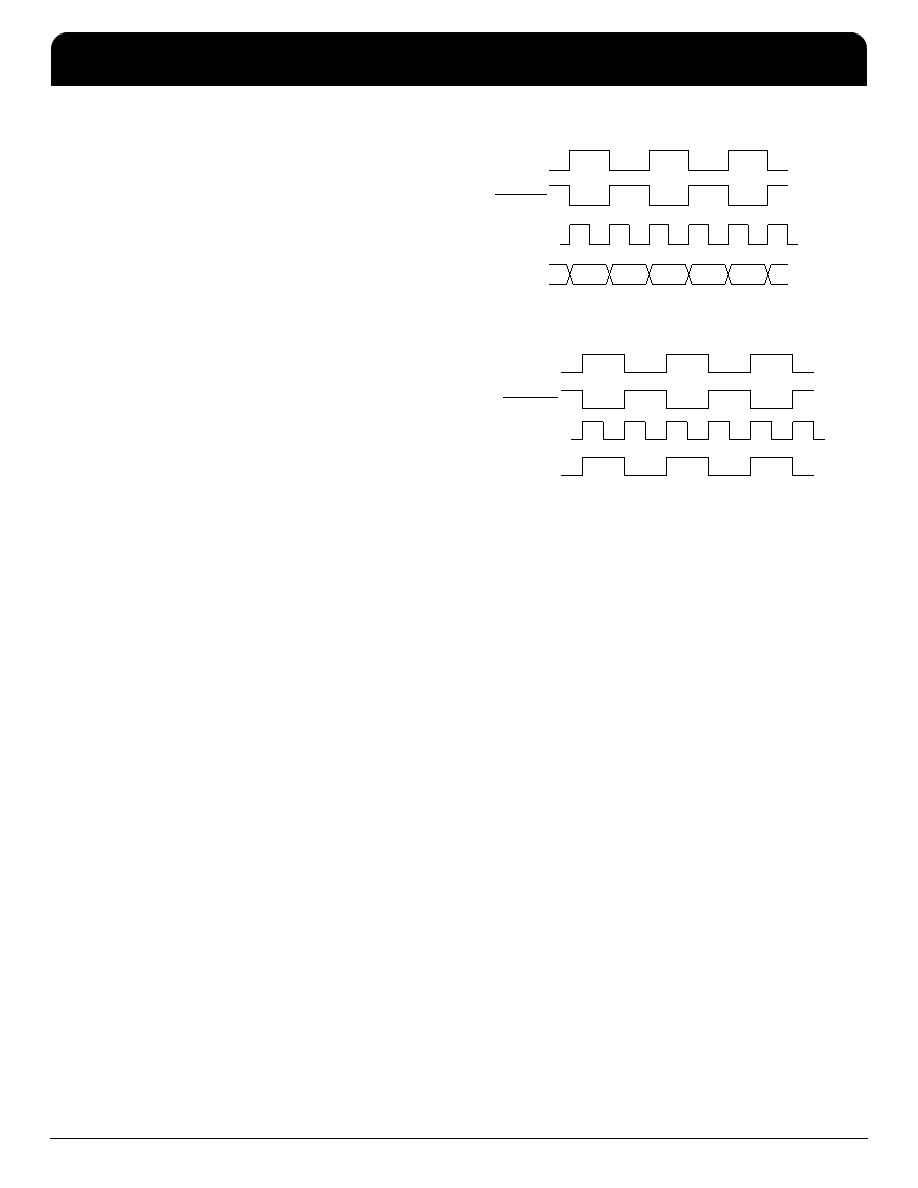
Next, the feedback scheme should be chosen. If CLK2
is being used as a SYNC pulse, or is tri-stated, then
CLK1 must be connected to FBIN. If CLK2 is selected
to be CLK1/2 (DIV2=1, OECLK2=1) then either CLK1
or CLK2 must be connected to FBIN. The choice
between CLK1 or CLK2 is illustrated by the following
examples where the device has been configured to
generate CLK1 that is twice the frequency on PECLIN.
Using CLK1 as feedback will always result in
synchronized rising edges between PECLIN and CLK1
if CLK1 is used as feedback. CLK2 could be a falling
edge compared to PECLIN. Therefore, wherever
possible it is recommended to use CLK2 for feedback,
which will synchronize the rising edges of all three
clocks.
More complicated feedback schemes can be used,
such as incorporating multiple output buffers in the
feedback path. An example is given later in the
datasheet. The fundamental property of the ICS527-02
is that it aligns rising edges on PECLIN and FBIN at a
ratio determined by the reference and feedback
dividers.
Set S1 and S0 (page 2) based on the output frequency.
Lastly, the divider settings should be selected. This is
described in the following section.
Determining ICS527-02 Divider Settings
The user has full control in setting the desired output
clock over the range shown in the table on page 2. The
user should connect the divider select input pins
directly to ground (or VDD, although this is not required
because of internal pull-ups) during Printed Circuit
Board layout, so the ICS527-02 automatically produces
PE C L IN
C L K 1 F eedbac k
CL K 1
CL K 2
ph as e is
in d e t e r m in a t e
PE C L IN
PE C L I N
CL K 1
CL K 2
C L K 2 F eed bac k
PE C L I N
ICS527-02
Clock Slicer User Configurable PECL Input Zero Delay Buffer
TSD
IDT / ICS Clock Slicer User Configurable PECL Input Zero Delay Buffer
ICS527-02
3
相关PDF资料 |
PDF描述 |
|---|---|
| ICS527R-02T | 527 SERIES, PLL BASED CLOCK DRIVER, 2 TRUE OUTPUT(S), 0 INVERTED OUTPUT(S), PDSO28 |
| ICS527R-02 | 527 SERIES, PLL BASED CLOCK DRIVER, 2 TRUE OUTPUT(S), 0 INVERTED OUTPUT(S), PDSO28 |
| ICS527R-04LF | 527 SERIES, PLL BASED CLOCK DRIVER, 1 TRUE OUTPUT(S), 0 INVERTED OUTPUT(S), PDSO28 |
| ICS527R-04T | 527 SERIES, PLL BASED CLOCK DRIVER, 1 TRUE OUTPUT(S), 0 INVERTED OUTPUT(S), PDSO28 |
| ICS527R-04 | 527 SERIES, PLL BASED CLOCK DRIVER, 1 TRUE OUTPUT(S), 0 INVERTED OUTPUT(S), PDSO28 |
相关代理商/技术参数 |
参数描述 |
|---|---|
| ICS527R-02ILF | 制造商:Integrated Device Technology Inc 功能描述:IC CLOCK SLICER ZD BUFFER 28SSOP |
| ICS527R-02ILFT | 制造商:Integrated Device Technology Inc 功能描述:IC CLOCK SLICER ZD BUFFER 28SSOP |
| ICS527R-02IT | 功能描述:IC CLOCK SLICER ZD BUFFER 28SSOP RoHS:否 类别:集成电路 (IC) >> 时钟/计时 - 时钟发生器,PLL,频率合成器 系列:- 标准包装:1,000 系列:- 类型:时钟/频率合成器,扇出分配 PLL:- 输入:- 输出:- 电路数:- 比率 - 输入:输出:- 差分 - 输入:输出:- 频率 - 最大:- 除法器/乘法器:- 电源电压:- 工作温度:- 安装类型:表面贴装 封装/外壳:56-VFQFN 裸露焊盘 供应商设备封装:56-VFQFP-EP(8x8) 包装:带卷 (TR) 其它名称:844S012AKI-01LFT |
| ICS527R-02LF | 功能描述:IC CLK SLICER ZDB CONFIG 28-SSOP RoHS:是 类别:集成电路 (IC) >> 时钟/计时 - 时钟发生器,PLL,频率合成器 系列:- 标准包装:1,000 系列:- 类型:时钟/频率合成器,扇出分配 PLL:- 输入:- 输出:- 电路数:- 比率 - 输入:输出:- 差分 - 输入:输出:- 频率 - 最大:- 除法器/乘法器:- 电源电压:- 工作温度:- 安装类型:表面贴装 封装/外壳:56-VFQFN 裸露焊盘 供应商设备封装:56-VFQFP-EP(8x8) 包装:带卷 (TR) 其它名称:844S012AKI-01LFT |
| ICS527R-02LFT | 功能描述:IC CLOCK SLICER ZD BUFFER 28SSOP RoHS:是 类别:集成电路 (IC) >> 时钟/计时 - 时钟发生器,PLL,频率合成器 系列:- 标准包装:1,000 系列:- 类型:时钟/频率合成器,扇出分配 PLL:- 输入:- 输出:- 电路数:- 比率 - 输入:输出:- 差分 - 输入:输出:- 频率 - 最大:- 除法器/乘法器:- 电源电压:- 工作温度:- 安装类型:表面贴装 封装/外壳:56-VFQFN 裸露焊盘 供应商设备封装:56-VFQFP-EP(8x8) 包装:带卷 (TR) 其它名称:844S012AKI-01LFT |
发布紧急采购,3分钟左右您将得到回复。