- 您现在的位置:买卖IC网 > PDF目录8758 > ICS542MLFT (IDT, Integrated Device Technology Inc)IC CLOCK BUFF DIVIDER 1:2 8-SOIC PDF资料下载
参数资料
| 型号: | ICS542MLFT |
| 厂商: | IDT, Integrated Device Technology Inc |
| 文件页数: | 2/6页 |
| 文件大小: | 0K |
| 描述: | IC CLOCK BUFF DIVIDER 1:2 8-SOIC |
| 标准包装: | 1 |
| 类型: | 扇出缓冲器(分配),除法器 |
| 电路数: | 1 |
| 比率 - 输入:输出: | 1:2 |
| 差分 - 输入:输出: | 无/无 |
| 输入: | CMOS |
| 输出: | 三态,CMOS |
| 频率 - 最大: | 156MHz |
| 电源电压: | 3 V ~ 5.5 V |
| 工作温度: | 0°C ~ 70°C |
| 安装类型: | 表面贴装 |
| 封装/外壳: | 8-SOIC(0.154",3.90mm 宽) |
| 供应商设备封装: | 8-SOIC |
| 包装: | 标准包装 |
| 产品目录页面: | 1251 (CN2011-ZH PDF) |
| 其它名称: | 800-1803-6 |
ICS542
CLOCK DIVIDER
IDT / ICS CLOCK DIVIDER
2
ICS542
REV J 051310
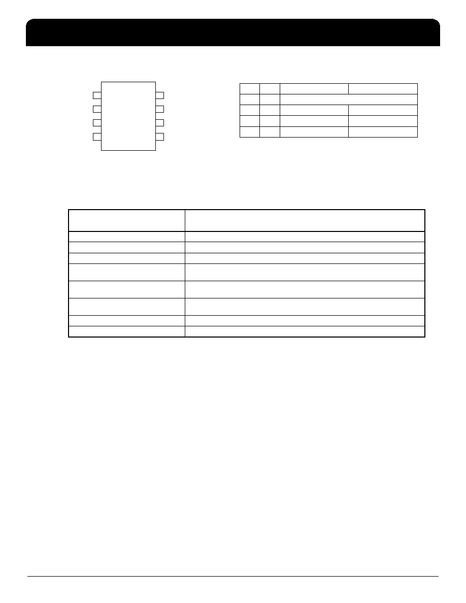
Pin Assignment
8-pin (150 mil) SOIC
Clock Decoding Table
0 = connect directly to ground
1 = connect directly to VDD
Pin Descriptions
External Components
Series Termination Resistor
Clock output traces over one inch should use series
termination. To series terminate a 50
trace (a commonly
used trace impedance), place a 33
resistor in series with
the clock line, as close to the clock output pin as possible.
The nominal impedance of the clock output is 20
.
Decoupling Capacitor
As with any high-performance mixed-signal IC, the ICS542
must be isolated from system power supply noise to perform
optimally.
A decoupling capacitor of 0.01F must be connected
between VDD and the PCB ground plane.
PCB Layout Recommendations
For optimum device performance and lowest output phase
noise, the following guidelines should be observed.
1) The 0.01F decoupling capacitor should be mounted on
the component side of the board as close to the VDD pin as
possible. No vias should be used between decoupling
capacitor and VDD pin. The PCB trace to VDD pin should
be kept as short as possible, as should the PCB trace to the
ground via. Distance of the ferrite bead and bulk decoupling
from the device is less critical.
2) To minimize EMI, the 33
series termination resistor (if
needed) should be placed close to the clock output.
3) An optimum layout is one with all components on the
ICLK
VDD
GND
CLK/ 2
S0
OE
S1
CLK
1
2
3
4
8
7
6
5
S1
S0
CLK
CLK/2
00
Power Down All
0
1
Input/6
Input/12
1
0
Input/8
Input/16
1
Input/2
Input/4
Pin
Number
Pin
Name
Pin
Type
Pin Description
1
ICLK
XI
Clock input.
2
VDD
Power
Connect to +3.3 V or +5 V.
3
GND
Power
Connect to ground.
4
S0
Input
Select 0 for output clock. Connect to GND or VDD, per decoding table above.
Internal pull-up resistor.
5
S1
Input
Select 1 for output clock. Connect to GND or VDD, per decoding table above.
Internal pull-up resistor.
6
OE
Input
Output Enable. Tri-states both output clocks when low. Internal pull-up
resistor.
7
CLK/2
Output
Clock output per table above. Low skew divide by two of pin 8 clock.
8
CLK
Output
Clock output per table above.
相关PDF资料 |
PDF描述 |
|---|---|
| VI-J33-MZ-F3 | CONVERTER MOD DC/DC 24V 25W |
| SI5330F-A00214-GM | IC CLK BUFFER TRANSLA 1:8 24-QFN |
| ICS83905AGILFT | IC CLK BUFF 1:6 100MHZ 16-TSSOP |
| IDT49FCT3805PYG | IC CLK BUFFER 1:5 100MHZ 20-SSOP |
| ICS551MILFT | IC CLK BUFFER 1:4 160MHZ 8-SOIC |
相关代理商/技术参数 |
参数描述 |
|---|---|
| ICS542MT | 功能描述:IC CLOCK BUFF DIVIDER 1:2 8-SOIC RoHS:否 类别:集成电路 (IC) >> 时钟/计时 - 时钟缓冲器,驱动器 系列:- 标准包装:1 系列:HiPerClockS™ 类型:扇出缓冲器(分配),多路复用器 电路数:1 比率 - 输入:输出:2:18 差分 - 输入:输出:是/无 输入:CML,LVCMOS,LVPECL,LVTTL,SSTL 输出:LVCMOS,LVTTL 频率 - 最大:250MHz 电源电压:2.375 V ~ 3.465 V 工作温度:0°C ~ 70°C 安装类型:表面贴装 封装/外壳:32-LQFP 供应商设备封装:32-TQFP(7x7) 包装:- 其它名称:800-1923-6 |
| ICS543 | 制造商:ICS 制造商全称:ICS 功能描述:PRELIMINARY INFORMATION Clock Divider and 2X Multiplier |
| ICS543M | 制造商:ICS 制造商全称:ICS 功能描述:PRELIMINARY INFORMATION Clock Divider and 2X Multiplier |
| ICS543MT | 制造商:ICS 功能描述: |
| ICS544-01 | 制造商:ICS 制造商全称:ICS 功能描述:Clock Divider |
发布紧急采购,3分钟左右您将得到回复。