- 您现在的位置:买卖IC网 > PDF目录67109 > ICS554G-01T (INTEGRATED DEVICE TECHNOLOGY INC) LOW SKEW CLOCK DRIVER, 4 TRUE OUTPUT(S), 0 INVERTED OUTPUT(S), PDSO16 PDF资料下载
参数资料
| 型号: | ICS554G-01T |
| 厂商: | INTEGRATED DEVICE TECHNOLOGY INC |
| 元件分类: | 时钟及定时 |
| 英文描述: | LOW SKEW CLOCK DRIVER, 4 TRUE OUTPUT(S), 0 INVERTED OUTPUT(S), PDSO16 |
| 封装: | 0.173 INCH, 0.65 MM PITCH, TSSOP-16 |
| 文件页数: | 3/5页 |
| 文件大小: | 67K |
| 代理商: | ICS554G-01T |
LOW SKEW 1 TO 4 CLOCK BUFFER PECL IN, PECL OUT
MDS 554-01 B
3
Revision 052501
Int egrat ed C i rcuit Syste ms q 525 R a ce S t r eet, San Jose, CA 95126 q t e l (40 8 ) 295 -9800 q
w w w. icst . c om
ICS554-01
External Components
The ICS554-01 requires a decoupling capacitor of 0.01
F to be connected between VDD on pin 2 and
GND on pin 7, as well as between VDD on pin 15 and GND on pin 10. These decoupling capacitors should
be placed as close to the device as possible. A 0.01
F capacitor must be placed between the RES (pin 16)
and Ground, also, a resistor must be connected between the RES (pin 16) and VDD. Another eight
resistors are needed for the PECL outputs as shown on the block diagram on page 1. Suggested values of
these resistors are shown in the Block Diagram, but they can be varied to change the differential pair
output swing, and the DC level. Refer to Application Note, MAN09.
To achieve the low output skews that the ICS554-01 is capable of, careful attention must be paid to board
layout. Essentially, all 8 outputs must have identical terminations, loads, and trace geometries. If they do
not, the output skew will be degraded. For example, using a 30
series termination on one output (with
33
on the others) will cause at least 15ps of skew.
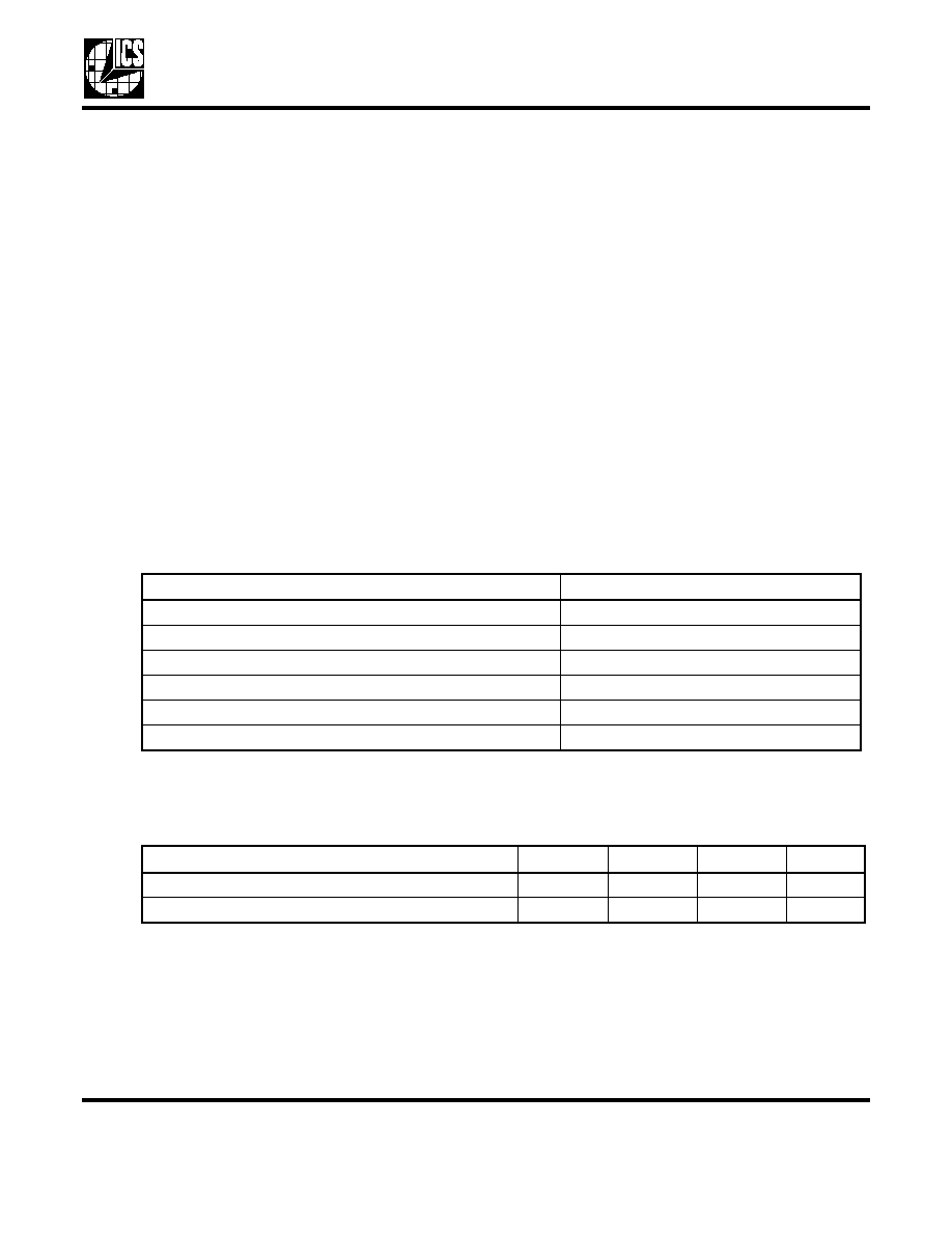
Absolute Maximum Ratings
Stresses above the ratings listed below can cause permanent damage to the ICS554-01. These ratings,
which are standard values for ICS commercially rated parts, are stress ratings only. Functional operation of
the device at these or any other conditions above those indicated in the operational sections of the
specifications is not implied. Exposure to absolute maximum rating conditions for extended periods can
affect product reliability. Electrical parameters are guaranteed only over the recommended operating
temperature range.
Recommended Operation Conditions
Item
Rating
Supply Voltage, VDD
7V
All Inputs and Outputs
-0.5V to VDD+0.5V
Ambient Operating Temperature
0 to +70
°C
Storage Temperature
-65 to +150
°C
Junction Temperature
175
°C
Soldering Temperature
260
°C
Parameter
Min.
Typ.
Max.
Units
Ambient Operating Temperature
0
–+70
°C
Power Supply Voltage (measured in respect to GND)
+3.15
+5.25
V
相关PDF资料 |
PDF描述 |
|---|---|
| ICS558G-01T | 558 SERIES, LOW SKEW CLOCK DRIVER, 4 TRUE OUTPUT(S), 0 INVERTED OUTPUT(S), PDSO16 |
| ICS558G-01 | 558 SERIES, LOW SKEW CLOCK DRIVER, 4 TRUE OUTPUT(S), 0 INVERTED OUTPUT(S), PDSO16 |
| ICS580M-01 | 580 SERIES, LOW SKEW CLOCK DRIVER, 2 TRUE OUTPUT(S), 0 INVERTED OUTPUT(S), PDSO16 |
| ICS580M-01ILF | 580 SERIES, LOW SKEW CLOCK DRIVER, 2 TRUE OUTPUT(S), 0 INVERTED OUTPUT(S), PDSO16 |
| ICS581G-01LFT | 581 SERIES, PLL BASED CLOCK DRIVER, 4 TRUE OUTPUT(S), 0 INVERTED OUTPUT(S), PDSO16 |
相关代理商/技术参数 |
参数描述 |
|---|---|
| ICS554GI-01A | 制造商:ICS 制造商全称:ICS 功能描述:LOW SKEW 1 TO 4 CLOCK BUFFER PECL IN, PECL OUT |
| ICS554GI-01AT | 制造商:ICS 制造商全称:ICS 功能描述:LOW SKEW 1 TO 4 CLOCK BUFFER PECL IN, PECL OUT |
| ICS556-01 | 制造商:ICS 制造商全称:ICS 功能描述:BROADCOM 25 MHZ LVDS CLOCK |
| ICS556-03 | 制造商:ICS 制造商全称:ICS 功能描述:QUAD LVDS OSCILLATOR/BUFFER |
| ICS556-03I | 制造商:ICS 制造商全称:ICS 功能描述:QUAD LVDS OSCILLATOR/BUFFER |
发布紧急采购,3分钟左右您将得到回复。