- 您现在的位置:买卖IC网 > PDF目录67685 > ICS557MI-01LFT (INTEGRATED DEVICE TECHNOLOGY INC) 100 MHz, PROC SPECIFIC CLOCK GENERATOR, PDSO8 PDF资料下载
参数资料
| 型号: | ICS557MI-01LFT |
| 厂商: | INTEGRATED DEVICE TECHNOLOGY INC |
| 元件分类: | 时钟产生/分配 |
| 英文描述: | 100 MHz, PROC SPECIFIC CLOCK GENERATOR, PDSO8 |
| 封装: | 0.150 INCH, GREEN, SOIC-8 |
| 文件页数: | 5/11页 |
| 文件大小: | 255K |
| 代理商: | ICS557MI-01LFT |
ICS557-01
PCI-EXPRESS CLOCK SOURCE
PCIE SSCG
IDT / ICS PCI-EXPRESS CLOCK SOURCE
3
ICS557-01
REV H 062607
Applications Information
External Components
A minimum number of external components are required for
proper operation.
Decoupling Capacitors
Decoupling capacitors of 0.01
F should be connected
between VDD and the ground plane (pin 4) as close to the
VDD pin as possible. Do not share ground vias between
components. Route power from power source through the
capacitor pad and then into ICS pin.
Crystal
A 25 MHz fundamental mode parallel resonant crystal with
CL = 16 pF should be used. This crystal must have less than
300 ppm of error across temperature in order for the
ICS557-01 to meet PCI Express specifications.
Crystal Capacitors
Crystal capacitors are connected from pins X1 to ground
and X2 to ground to optimize the accuracy of the output
frequency.
CL= Crystal’s load capacitance in pF
Crystal Capacitors (pF) = (CL- 8) * 2
For example, for a crystal with a 16 pF load cap, each
external crystal cap would be 16 pF. (16-8)*2=16.
Current Source (Iref) Reference Resistor - RR
If board target trace impedance (Z) is 50
, then R
R = 475
(1%), providing IREF of 2.32 mA. The output current (IOH) is
equal to 6*IREF.
Output Termination
The PCI-Express differential clock outputs of the ICS557-01
are open source drivers and require an external series
resistor and a resistor to ground. These resistor values and
their allowable locations are shown in detail in the
PCI-Express Layout Guidelines section.
The ICS557-01can also be configured for LVDS compatible
voltage levels. See the LVDS Compatible Layout Guidelines
section
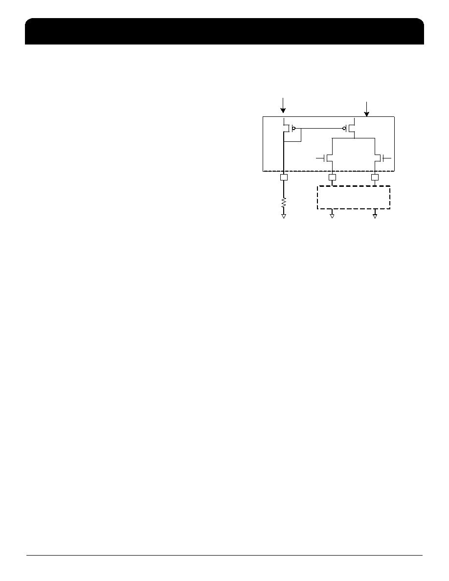
Output Structures
General PCB Layout Recommendations
For optimum device performance and lowest output phase
noise, the following guidelines should be observed.
1. Each 0.01F decoupling capacitor should be mounted on
the component side of the board as close to the VDD pin as
possible.
2. No vias should be used between decoupling capacitor
and VDD pin.
3. The PCB trace to VDD pin should be kept as short as
possible, as should the PCB trace to the ground via.
Distance of the ferrite bead and bulk decoupling from the
device is less critical.
4. An optimum layout is one with all components on the
same side of the board, minimizing vias through other signal
layers (any ferrite beads and bulk decoupling capacitors can
be mounted on the back). Other signal traces should be
routed away from the ICS557-01.This includes signal traces
just underneath the device, or on layers adjacent to the
ground plane layer used by the device.
R
R 475
6*IREF
=2.3 mA
IREF
See Output Termination
Sections - Pages 3 ~ 5
W
相关PDF资料 |
PDF描述 |
|---|---|
| ICS570A | 570 SERIES, PLL BASED CLOCK DRIVER, 2 TRUE OUTPUT(S), 0 INVERTED OUTPUT(S), PDSO8 |
| ICS570AILF | 570 SERIES, PLL BASED CLOCK DRIVER, 2 TRUE OUTPUT(S), 0 INVERTED OUTPUT(S), PDSO8 |
| ICS570MI | 570 SERIES, PLL BASED CLOCK DRIVER, 2 TRUE OUTPUT(S), 0 INVERTED OUTPUT(S), PDSO8 |
| ICS570MLF | 570 SERIES, PLL BASED CLOCK DRIVER, 2 TRUE OUTPUT(S), 0 INVERTED OUTPUT(S), PDSO8 |
| ICS570AT | 570 SERIES, PLL BASED CLOCK DRIVER, 2 TRUE OUTPUT(S), 0 INVERTED OUTPUT(S), PDSO8 |
相关代理商/技术参数 |
参数描述 |
|---|---|
| ICS557MI-01T | 制造商:ICS 制造商全称:ICS 功能描述:PCI-EXPRESS CLOCK SOURCE |
| ICS558-01 | 制造商:ICS 制造商全称:ICS 功能描述:PECL/CMOS TO CMOS CLOCK DIVIDER |
| ICS558-02 | 制造商:ICS 制造商全称:ICS 功能描述:LVHSTL TO CMOS CLOCK DIVIDER |
| ICS558AG-02 | 功能描述:IC CLK BUFF DIVIDER 1:4 16-TSSOP RoHS:否 类别:集成电路 (IC) >> 时钟/计时 - 时钟缓冲器,驱动器 系列:ClockBlocks™ 标准包装:1 系列:HiPerClockS™ 类型:扇出缓冲器(分配),多路复用器 电路数:1 比率 - 输入:输出:2:18 差分 - 输入:输出:是/无 输入:CML,LVCMOS,LVPECL,LVTTL,SSTL 输出:LVCMOS,LVTTL 频率 - 最大:250MHz 电源电压:2.375 V ~ 3.465 V 工作温度:0°C ~ 70°C 安装类型:表面贴装 封装/外壳:32-LQFP 供应商设备封装:32-TQFP(7x7) 包装:- 其它名称:800-1923-6 |
| ICS558AG-02LN | 功能描述:IC CLK BUFF DIVIDER 1:4 16-TSSOP RoHS:是 类别:集成电路 (IC) >> 时钟/计时 - 时钟缓冲器,驱动器 系列:ClockBlocks™ 标准包装:74 系列:- 类型:扇出缓冲器(分配) 电路数:1 比率 - 输入:输出:1:10 差分 - 输入:输出:是/是 输入:HCSL, LVCMOS, LVDS, LVPECL, LVTTL 输出:HCSL,LVDS 频率 - 最大:400MHz 电源电压:3 V ~ 3.6 V 工作温度:-40°C ~ 85°C 安装类型:表面贴装 封装/外壳:32-VFQFN 裸露焊盘 供应商设备封装:32-QFN(5x5) 包装:管件 |
发布紧急采购,3分钟左右您将得到回复。