- 您现在的位置:买卖IC网 > PDF目录9047 > ICS663MLFT (IDT, Integrated Device Technology Inc)IC PLL BUILDING BLOCK 8-SOIC PDF资料下载
参数资料
| 型号: | ICS663MLFT |
| 厂商: | IDT, Integrated Device Technology Inc |
| 文件页数: | 5/8页 |
| 文件大小: | 0K |
| 描述: | IC PLL BUILDING BLOCK 8-SOIC |
| 标准包装: | 2,500 |
| 类型: | 锁相环路(PLL) |
| PLL: | 是 |
| 输入: | CMOS |
| 输出: | CMOS |
| 电路数: | 1 |
| 比率 - 输入:输出: | 1:1 |
| 差分 - 输入:输出: | 无/无 |
| 频率 - 最大: | 120MHz |
| 除法器/乘法器: | 是/无 |
| 电源电压: | 3.13 V ~ 5.5 V |
| 工作温度: | 0°C ~ 70°C |
| 安装类型: | 表面贴装 |
| 封装/外壳: | 8-SOIC(0.154",3.90mm 宽) |
| 供应商设备封装: | 8-SOIC |
| 包装: | 带卷 (TR) |
| 其它名称: | 663MLFT |
ICS663
PLL BUILDING BLOCK
IDT / ICS PLL BUILDING BLOCK
5
ICS663
REV E 012006
External Components
The ICS663 requires a minimum number of external
components for proper operation. A decoupling capacitor of
0.01
F should be connected between VDD and GND as
close to the ICS663 as possible. A series termination
resistor of 33
may be used at the clock output.
Special considerations must be made in choosing loop
components C1 and C2:
1) The loop capacitors should be a low-leakage type to
avoid leakage-induced phase noise. For this reason, DO
NOT use any type of polarized or electrolytic capacitors.
2) Microphonics (mechanical board vibration) can also
induce output phase noise when the loop bandwidth is less
than 1 kHz. For this reason, ceramic capacitors should have
C0G or NP0 dielectric. Avoid high-K dielectrics like Z5U and
X7R. These and some other ceramics have piezoelectric
properties that convert mechanical vibration into voltage
noise that interferes with VCXO operation.
For larger loop capacitor values such as 0.1
F or 1F, PPS
film types made by Panasonic, or metal poly types made by
Murata or Cornell Dubilier are recommended.
For questions or changes regarding loop filter
characteristics, please contact your sales area FAE, or IDT
Applications.
Avoiding PLL Lockup
In some applications, the ICS663 can “lock up” at the
maximum VCO frequency. The way to avoid this problem is
to use an external divider that always operates correctly
regardless of the CLK output frequency. The CLK output
frequency may be up to 2x the maximum Output Clock
Frequency listed in the AC Electrical Characteristics above
when the device is in an unlocked condition. Make sure that
the external divider can operate up to this frequency.
Explanation of Operation
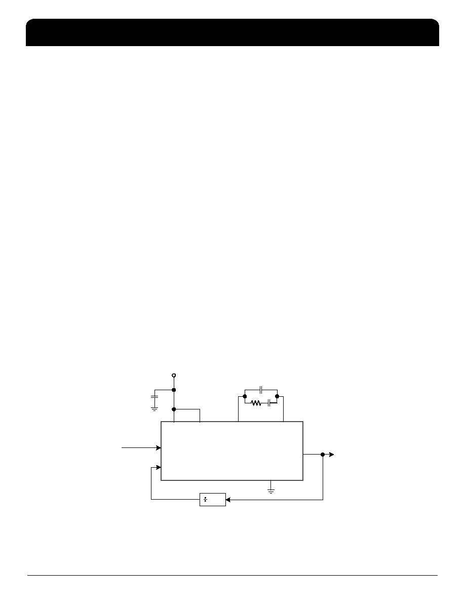
The ICS663 is a PLL building block circuit that includes an
integrated VCO with a wide operating range. The device
uses external PLL loop filter components which through
proper configuration allow for low input clock reference
frequencies, such as a 15.7 kHz Hsync input.
The phase/frequency detector compares the falling edges of
the clocks inputted to FBIN and REFIN. It then generates an
error signal to the charge pump, which produces a charge
proportional to this error. The external loop filter integrates
this charge, producing a voltage that then controls the
frequency of the VCO. This process continues until the
edges of FBIN are aligned with the edges of the REFIN
clock, at which point the output frequency will be locked to
the input frequency.
Figure 1. Example Configuration -- Generating a 20 MHz clock from a 200 kHz reference
RE F IN
+ 3 .3 or 5 V
VDD
S E L
0.01
F
FBIN
200 kH z
100
D igital D iv ider such as
IC S 674-01
GN D
CLK
LF R
20 M H z
LF
C
1
R
Z
C
2
200 kH z
IC S 663
相关PDF资料 |
PDF描述 |
|---|---|
| DS1666-10+ | IC DIG POT 10K 14-DIP |
| MAX5489ETE#TG16 | IC POT DGTL DUAL 256-TAP 16-TQFN |
| MAX5487ETE+T | IC POT DGTL DUAL 256-TAP 16-TQFN |
| MAX5488ETE#TG16 | IC POT DGTL DUAL 256-TAP 16-TQFN |
| MAX5487ETE#G16 | IC POT DGTL DUAL 256-TAP 16-TQFN |
相关代理商/技术参数 |
参数描述 |
|---|---|
| ICS663MT | 功能描述:IC PLL BUILDING BLOCK 8-SOIC RoHS:否 类别:集成电路 (IC) >> 时钟/计时 - 时钟发生器,PLL,频率合成器 系列:- 产品变化通告:Product Discontinuation 04/May/2011 标准包装:96 系列:- 类型:时钟倍频器,零延迟缓冲器 PLL:带旁路 输入:LVTTL 输出:LVTTL 电路数:1 比率 - 输入:输出:1:8 差分 - 输入:输出:无/无 频率 - 最大:133.3MHz 除法器/乘法器:是/无 电源电压:3 V ~ 3.6 V 工作温度:0°C ~ 70°C 安装类型:表面贴装 封装/外壳:16-TSSOP(0.173",4.40mm 宽) 供应商设备封装:16-TSSOP 包装:管件 其它名称:23S08-5HPGG |
| ICS664-01 | 制造商:ICS 制造商全称:ICS 功能描述:Digital Video Clock Source |
| ICS664-02 | 制造商:ICS 制造商全称:ICS 功能描述:PECL Digital Video Clock Source |
| ICS664-03 | 制造商:ICS 制造商全称:ICS 功能描述:Digital Video Clock Source |
| ICS664-03LF | 制造商:ICS 制造商全称:ICS 功能描述:Digital Video Clock Source |
发布紧急采购,3分钟左右您将得到回复。