- 您现在的位置:买卖IC网 > PDF目录67110 > ICS670M-04IT 670 SERIES, PLL BASED CLOCK DRIVER, 1 TRUE OUTPUT(S), 0 INVERTED OUTPUT(S), PDSO16 PDF资料下载
参数资料
| 型号: | ICS670M-04IT |
| 元件分类: | 时钟及定时 |
| 英文描述: | 670 SERIES, PLL BASED CLOCK DRIVER, 1 TRUE OUTPUT(S), 0 INVERTED OUTPUT(S), PDSO16 |
| 封装: | 0.150 INCH, SOIC-16 |
| 文件页数: | 1/6页 |
| 文件大小: | 171K |
| 代理商: | ICS670M-04IT |
ICS670-04
MDS 670-04 B
1
Revision 011905
Integrated Circuit Systems l 525 Race Street, San Jose, CA 95126 l tel (408) 297-1201 l
www.icst.com
LOW PHASE NOISE, ZERO DELAY BUFFER AND MULTIPLIER
Description
The ICS670-04 is a high speed, low phase noise, Zero
Delay Buffer (ZDB) which integrates ICS’ proprietary
analog/digital Phase Locked Loop (PLL) techniques. It
is identical to the ICS670-02, but with an increased
maximum output frequency of 210 MHz. Part of ICS’
ClockBlocksTM family, the part’s zero delay feature
means that the rising edge of the input clock aligns with
the rising edges of the outputs giving the appearance of
no delay through the device. There are two identical
outputs on the chip. The FBCLK should be used to
connect to the FBIN. Each output has its own output
enable pin.
The ICS670-04 is ideal for synchronizing outputs in a
large variety of systems, from personal computers to
data communications to video. By allowing off-chip
feedback paths, the chip can eliminate the delay
through other devices. The 15 different on-chip
multipliers work in a variety of applications. For other
multipliers, including functional multipliers, see the
ICS527.
Features
Packaged in 16-pin SOIC Pb (lead) free
Clock inputs from 5 to 210 MHz (see page 2)
Patented PLL with low phase noise
Output clocks up to 210 MHz at 3.3 V
15 selectable on-chip multipliers
Power down mode available
Low phase noise: -111 dBc/Hz at 10 kHz
Output enable function tri-states outputs
Low jitter 15 ps one sigma
Advanced, low power, sub-micron CMOS process
Operating voltage of 3.3 V or 5 V
Industrial temperature grade
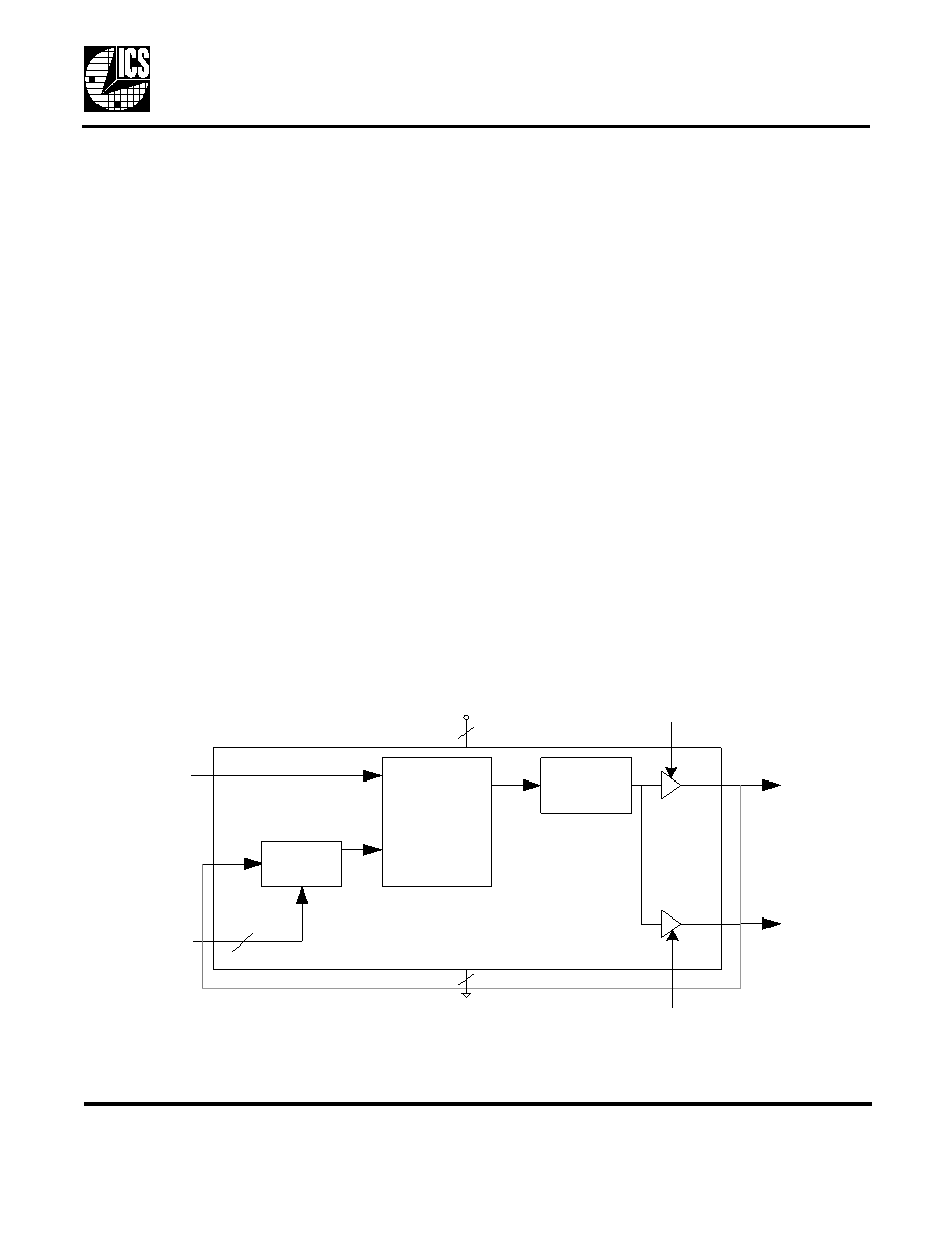
Block Diagram
Divide by
N
Voltage
Controlled
Oscillator
FB C L K
OE 1
Phase
Detector,
Charge
Pump, and
Loop Filter
FB I N
S3 :S 0
IC L K
CL K2
4
OE 2
VDD
3
GND
3
E x te rn al Fe ed ba ck f r om FB C L K is r e com m e nd ed .
相关PDF资料 |
PDF描述 |
|---|---|
| ICS671G-15LFT | PLL BASED CLOCK DRIVER, 8 TRUE OUTPUT(S), 0 INVERTED OUTPUT(S), PDSO24 |
| ICS671G-15T | PLL BASED CLOCK DRIVER, 8 TRUE OUTPUT(S), 0 INVERTED OUTPUT(S), PDSO24 |
| ICS672M-01T | 672 SERIES, PLL BASED CLOCK DRIVER, 4 TRUE OUTPUT(S), 0 INVERTED OUTPUT(S), PDSO16 |
| ICS672MI-02LF | 672 SERIES, PLL BASED CLOCK DRIVER, 4 TRUE OUTPUT(S), 0 INVERTED OUTPUT(S), PDSO16 |
| ICS672M-02LFT | 672 SERIES, PLL BASED CLOCK DRIVER, 4 TRUE OUTPUT(S), 0 INVERTED OUTPUT(S), PDSO16 |
相关代理商/技术参数 |
参数描述 |
|---|---|
| ICS670MI-02 | 功能描述:IC BUFFER/MULTIPLIER ZD 16-SOIC RoHS:否 类别:集成电路 (IC) >> 时钟/计时 - 时钟发生器,PLL,频率合成器 系列:ClockBlocks™ 产品变化通告:Product Discontinuation 04/May/2011 标准包装:96 系列:- 类型:时钟倍频器,零延迟缓冲器 PLL:带旁路 输入:LVTTL 输出:LVTTL 电路数:1 比率 - 输入:输出:1:8 差分 - 输入:输出:无/无 频率 - 最大:133.3MHz 除法器/乘法器:是/无 电源电压:3 V ~ 3.6 V 工作温度:0°C ~ 70°C 安装类型:表面贴装 封装/外壳:16-TSSOP(0.173",4.40mm 宽) 供应商设备封装:16-TSSOP 包装:管件 其它名称:23S08-5HPGG |
| ICS670MI-02LF | 功能描述:IC BUFFER/MULTIPLIER ZD 16-SOIC RoHS:是 类别:集成电路 (IC) >> 时钟/计时 - 时钟发生器,PLL,频率合成器 系列:ClockBlocks™ 标准包装:1,000 系列:- 类型:时钟/频率合成器,扇出分配 PLL:- 输入:- 输出:- 电路数:- 比率 - 输入:输出:- 差分 - 输入:输出:- 频率 - 最大:- 除法器/乘法器:- 电源电压:- 工作温度:- 安装类型:表面贴装 封装/外壳:56-VFQFN 裸露焊盘 供应商设备封装:56-VFQFP-EP(8x8) 包装:带卷 (TR) 其它名称:844S012AKI-01LFT |
| ICS670MI-02LFT | 功能描述:IC BUFFER/MULTIPLIER ZD 16-SOIC RoHS:是 类别:集成电路 (IC) >> 时钟/计时 - 时钟发生器,PLL,频率合成器 系列:ClockBlocks™ 标准包装:1,000 系列:- 类型:时钟/频率合成器,扇出分配 PLL:- 输入:- 输出:- 电路数:- 比率 - 输入:输出:- 差分 - 输入:输出:- 频率 - 最大:- 除法器/乘法器:- 电源电压:- 工作温度:- 安装类型:表面贴装 封装/外壳:56-VFQFN 裸露焊盘 供应商设备封装:56-VFQFP-EP(8x8) 包装:带卷 (TR) 其它名称:844S012AKI-01LFT |
| ICS670MI-02T | 功能描述:IC BUFFER/MULTIPLIER ZD 16-SOIC RoHS:否 类别:集成电路 (IC) >> 时钟/计时 - 时钟发生器,PLL,频率合成器 系列:ClockBlocks™ 产品变化通告:Product Discontinuation 04/May/2011 标准包装:96 系列:- 类型:时钟倍频器,零延迟缓冲器 PLL:带旁路 输入:LVTTL 输出:LVTTL 电路数:1 比率 - 输入:输出:1:8 差分 - 输入:输出:无/无 频率 - 最大:133.3MHz 除法器/乘法器:是/无 电源电压:3 V ~ 3.6 V 工作温度:0°C ~ 70°C 安装类型:表面贴装 封装/外壳:16-TSSOP(0.173",4.40mm 宽) 供应商设备封装:16-TSSOP 包装:管件 其它名称:23S08-5HPGG |
| ICS67-1 | 制造商:Thomas & Betts 功能描述:INSULATED SERV.ENTR.SLEEVE 制造商:Thomas & Betts 功能描述:Cable Accessories Compression Splice Aluminum |
发布紧急采购,3分钟左右您将得到回复。