- 您现在的位置:买卖IC网 > PDF目录2072 > ICS841664AGILFT (IDT, Integrated Device Technology Inc)IC CLOCK GENERATOR 28-TSSOP PDF资料下载
参数资料
| 型号: | ICS841664AGILFT |
| 厂商: | IDT, Integrated Device Technology Inc |
| 文件页数: | 3/19页 |
| 文件大小: | 0K |
| 描述: | IC CLOCK GENERATOR 28-TSSOP |
| 标准包装: | 1,000 |
| 系列: | HiPerClockS™, FemtoClock™ |
| 类型: | 时钟发生器,扇出配送,多路复用器 |
| PLL: | 带旁路 |
| 输入: | LVCMOS,LVTTL,晶体 |
| 输出: | HCSL,LVCMOS,LVTTL |
| 电路数: | 1 |
| 比率 - 输入:输出: | 2:5 |
| 差分 - 输入:输出: | 无/是 |
| 频率 - 最大: | 156.25MHz |
| 除法器/乘法器: | 是/无 |
| 电源电压: | 3.135 V ~ 3.465 V |
| 工作温度: | -40°C ~ 85°C |
| 安装类型: | 表面贴装 |
| 封装/外壳: | 28-TSSOP(0.240",6.10mm 宽) |
| 供应商设备封装: | 28-TSSOP |
| 包装: | 带卷 (TR) |
| 其它名称: | 841664AGILFT |
ICS841664AGI REVISION A JULY 15, 2013
11
2013 Integrated Device Technology, Inc.
ICS841664I Data Sheet
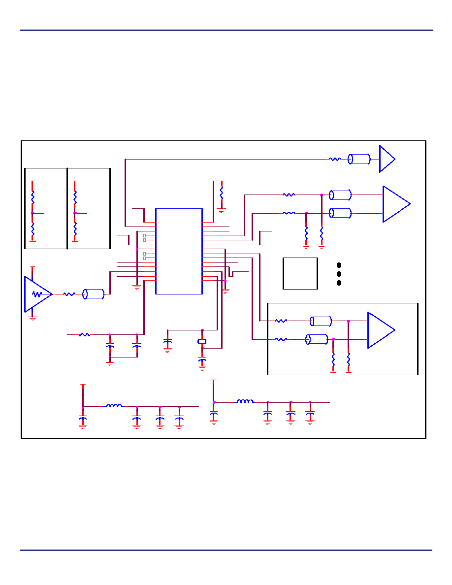
FEMTOCLOCK CRYSTAL-TO-HCSL CLOCK GENERATOR
Schematic Layout
Figure 1 shows an example of ICS841664I application schematic. In
this example, the device is operated at
VDD = VDDA = VDDOA =
VDDOB = 3.3V. The 18pF parallel resonant 25MHz crystal is used.
The load capacitance C1 = 27pF and C2 = 27pF are recommended
for frequency accuracy. Depending on the parasitic of the printed
circuit board layout, these values might require a slight adjustment to
optimize the frequency accuracy. Crystals with other load
capacitance specifications can be used. This will require
adjusting C1 and C2. For this device, the crystal load capacitors are
required for proper operation.
As with any high speed analog circuitry, the power supply pins are
vulnerable to random noise. To achieve optimum jitter performance,
power supply isolation is required. The ICS841664I provides
separate power supplies to isolate any high switching noise from
coupling into the internal PLL.
Figure 1. ICS841664I Schematic Example
In order to achieve the best possible filtering, it is recommended that
the placement of the filter components be on the device side of the
PCB as close to the power pins as possible. If space is limited, the
0.1F capacitor in each power pin filter should be placed on the
device side of the PCB and the other components can be placed on
the opposite side.
Power supply filter recommendations are a general guideline to be
used for reducing external noise from coupling into the devices. The
filter performance is designed for wide range of noise frequency. This
low-pass filter starts to attenuate noise at approximately 10kHz. If a
specific frequency noise component with high amplitude interference
is known, such as switching power supplies frequencies, it is
recommended that component values be adjusted and if required,
additional filtering be added. Additionally general design practice for
power plane voltage stability suggests adding bulk capacitances in
the general area of all devices.
The schematic example focuses on functional connections and is not
configuration specific. Refer to the pin description and functional
tables in the datasheet to ensure the logic control inputs are properly
set.
VD D
REF _I N
Zo = 50
HCSL Termination
FS EL1
C12
0.1uF
RE F_OU T
VDDA
MR/ nOE
R3
33
VDD
nQB 1
R5
50
Zo = 50
Set Logic
Input to
'0'
nQB0
VD D
R4
33
VDDOB=3.3V
QB1
R10
50
+
-
nR EF_OE
RU 2
Not Ins t all
R 8
0-33
C10
10uF
Zo = 50 Ohm
VDDOA=3.3V
HCSL Optional
Termination
RD 2
1K
Zo = 50
Ro ~ 7 Ohm
Q1
Driv er_LVC MOS
Logic Control Input Examples
BLM18BB221SN 2
Ferrit e Bead
1
2
C1
27pF
C8
0.1uF
(U1:6)
R 9
0-33
R6
50
C11
0. 1uF
Zo = 50
(U1:23)
VD D
FS EL0
VDDO
C7
0. 1uF
C9
0.1uF
3. 3V
R1
33
+
-
Optional
Set Logic
Input to
'1'
3. 3V
ToLogic
Input
pins
X1
25MH z
BLM18BB221SN1
F errit e Bead
1
2
VDD
C4
10u
R11
50
VDD=3.3V
ToLogic
Input
pins
R12
43
R7
10
LVC MOS
C3
0.1u
1 8 p F
REF_SEL
Recommended for PCI
Express Point-to-Point
Connection
Zo = 50
C6
10uF
VD D
(U1:18)
RD 1
Not Ins t all
VDDO
U1
1
2
3
4
5
14
6
7
8
9
10
11
15
16
17
18
19
20
21
22
23
24
12
13
28
27
26
25
VDD
REF _OU T
GN D
QA0
nQA0
VDD A
VDD OA
GN D
QA1
nQA1
nR EF_OE
BYP ASS
GN D
XTAL_OU T
XTAL_I N
VD D
MR /nOE
nQB1
QB1
GN D
VDDOB
nQB0
REF _I N
REF _SE L
IREF
FSEL0
FSEL1
QB0
C2
27pF
R2
475
(U1:1)
VDD
C5
0. 1uF
Recommended for PCI
Express Add-In Card
RU 1
1K
BY PA SS
VDDO
QB 0
相关PDF资料 |
PDF描述 |
|---|---|
| ICS8421002AGI-01LF | IC FREQ SYNTHESIZER 20-TSSOP |
| ICS843001CGILF | IC CLK GEN FIBRE CH 8TSSOP |
| ICS843002AG-01LFT | IC SYNTHESIZER LVPECL 20-TSSOP |
| ICS843002AKI-40LF | IC SYNTHESIZER LVPECL 32-VFQFPN |
| ICS843003AGI-01LF | IC SYNTHESIZER LVPECL 24-TSSOP |
相关代理商/技术参数 |
参数描述 |
|---|---|
| ICS841664I | 制造商:IDT 制造商全称:Integrated Device Technology 功能描述:FEMTOCLOCK? CRYSTAL-TO-HCSL CLOCK GENERATOR |
| ICS841N254AKILF | 功能描述:IC CLK SYNTH PLL 250MHZ 32VFQFN RoHS:是 类别:集成电路 (IC) >> 时钟/计时 - 时钟发生器,PLL,频率合成器 系列:FemtoClock® NG 标准包装:27 系列:Precision Edge® 类型:频率合成器 PLL:是 输入:PECL,晶体 输出:PECL 电路数:1 比率 - 输入:输出:1:1 差分 - 输入:输出:无/是 频率 - 最大:800MHz 除法器/乘法器:是/无 电源电压:3.135 V ~ 5.25 V 工作温度:0°C ~ 85°C 安装类型:表面贴装 封装/外壳:28-SOIC(0.295",7.50mm 宽) 供应商设备封装:28-SOIC 包装:管件 |
| ICS841N254AKILFT | 制造商:Integrated Device Technology Inc 功能描述:IC CLK SYNTHESIZER 32VFQFN |
| ICS841N254I | 制造商:IDT 制造商全称:Integrated Device Technology 功能描述:FEMTOCLOCK? NG Crystal-to-LVDS/HCSL Clock Synthesizer |
| ICS841S01 | 制造商:IDT 制造商全称:Integrated Device Technology 功能描述:PCI EXPRESS⑩ CLOCK GENERATOR |
发布紧急采购,3分钟左右您将得到回复。