- 您现在的位置:买卖IC网 > PDF目录8978 > ICS8422002AGILFT (IDT, Integrated Device Technology Inc)IC SYNTHESIZER LVHSTL 20-TSSOP PDF资料下载
参数资料
| 型号: | ICS8422002AGILFT |
| 厂商: | IDT, Integrated Device Technology Inc |
| 文件页数: | 12/16页 |
| 文件大小: | 0K |
| 描述: | IC SYNTHESIZER LVHSTL 20-TSSOP |
| 标准包装: | 2,500 |
| 系列: | HiPerClockS™, FemtoClock™ |
| 类型: | 频率合成器 |
| PLL: | 带旁路 |
| 输入: | LVCMOS,LVTTL,晶体 |
| 输出: | LVHSTL |
| 电路数: | 1 |
| 比率 - 输入:输出: | 2:2 |
| 差分 - 输入:输出: | 无/是 |
| 频率 - 最大: | 226.66MHz |
| 除法器/乘法器: | 是/是 |
| 电源电压: | 2.375 V ~ 3.465 V |
| 工作温度: | -40°C ~ 85°C |
| 安装类型: | 表面贴装 |
| 封装/外壳: | 20-TSSOP(0.173",4.40mm 宽) |
| 供应商设备封装: | 20-TSSOP |
| 包装: | 带卷 (TR) |
| 其它名称: | 8422002AGILFT |
ICS8422002AGI REVISION A AUGUST 12, 2009
5
2009 Integrated Device Technology, Inc.
ICS8422002I Data Sheet
FEMTOCLOCK CRYSTAL-TO-LVHSTL FREQUENCY SYNTHESIZER
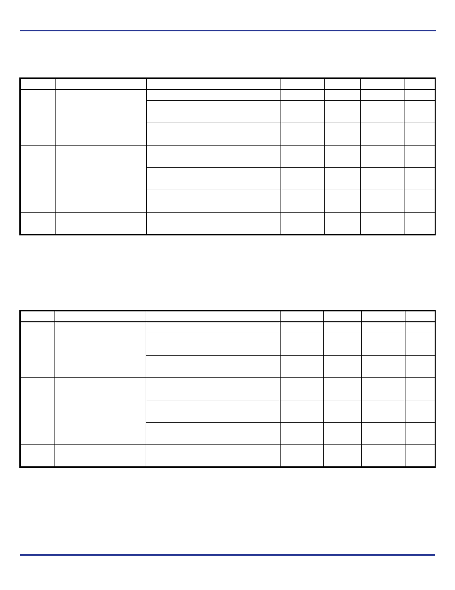
AC Electrical Characteristics
Table 5A. AC Characteristics, VDD = 3.3V ± 5%, VDDO = 1.8V ±0.2V, TA = -40°C to 85°C
NOTE: Electrical parameters are guaranteed over the specified ambient operating temperature range, which is established when the device is
mounted in a test socket with maintained transverse airflow greater than 500 lfpm. The device will meet specifications after thermal equilibrium
has been reached under these conditions.
NOTE 1: Defined as skew between outputs at the same supply voltages and with equal load conditions. Measured at VDDO/2.
NOTE 2: This parameter is defined in accordance with JEDEC Standard 65.
NOTE 3: Please refer to the Phase Noise Plot.
Table 5B. AC Characteristics, VDD = 2.5V ± 5%, VDDO = 1.8V ±0.2V, TA = -40°C to 85°C
NOTE: Electrical parameters are guaranteed over the specified ambient operating temperature range, which is established when the device is
mounted in a test socket with maintained transverse airflow greater than 500 lfpm. The device will meet specifications after thermal equilibrium
has been reached under these conditions.
NOTE 1: Defined as skew between outputs at the same supply voltages and with equal load conditions. Measured at VDDO/2.
NOTE 2: This parameter is defined in accordance with JEDEC Standard 65.
NOTE 3: Please refer to the Phase Noise Plot.
Symbol
Parameter
Test Conditions
Minimum
Typical
Maximum
Units
fOUT
Output Frequency
F_SEL[1:0] = 00
186.67
226.66
MHz
F_SEL[1:0] = 01
140
170
MHz
F_SEL[1:0] = 10
93.33
113.33
MHz
F_SEL[1:0] = 11
46.67
56.66
MHz
tsk(o)
Output Skew; NOTE 1, 2
35
ps
tjit()
RMS Phase Jitter (Random);
NOTE 3
212.5MHz, (637kHz – 10MHz)
0.59
ps
187.5MHz, (637kHz – 10MHz)
0.53
ps
159.375MHz, (637kHz – 10MHz)
0.56
ps
106.25MHz, (1.875MHz – 20MHz)
0.56
ps
53.125MHz, (637kHz – 10MHz)
0.66
ps
tR / tF
Output Rise/Fall Time
20% to 80%
275
875
ps
odc
Output Duty Cycle
N
≠ 348
52
%
N = 3
40
60
%
Symbol
Parameter
Test Conditions
Minimum
Typical
Maximum
Units
fOUT
Output Frequency
F_SEL[1:0] = 00
186.67
226.66
MHz
F_SEL[1:0] = 01
140
170
MHz
F_SEL[1:0] = 10
93.33
113.33
MHz
F_SEL[1:0] = 11
46.67
56.66
MHz
tsk(o)
Output Skew; NOTE 1, 2
35
ps
tjit()
RMS Phase Jitter (Random);
NOTE 3
212.5MHz, (637kHz – 10MHz)
0.60
ps
187.5MHz, (637kHz – 10MHz)
0.72
ps
159.375MHz, (637kHz – 10MHz)
0.64
ps
106.25MHz, (1.875MHz – 20MHz)
0.55
ps
53.125MHz, (637kHz – 10MHz)
0.68
ps
tR / tF
Output Rise/Fall Time
20% to 80%
250
650
ps
odc
Output Duty Cycle
N
≠ 348
52
%
N = 3
40
60
%
相关PDF资料 |
PDF描述 |
|---|---|
| ICS8421002AGILFT | IC FREQ SYNTHESIZER 20-TSSOP |
| ICS8421002AGI-01LFT | IC FREQ SYNTHESIZER 20-TSSOP |
| DAC8143FSZ | IC DAC 12BIT DAISY-CHAIN 16-SOIC |
| IDT74ALVC164245PAG8 | IC TRANSCVR TRI-ST 16BIT 48TSSOP |
| ICS843321AGI-12LFT | IC SYNTHESIZER CLK SONET 8TSSOP |
相关代理商/技术参数 |
参数描述 |
|---|---|
| ICS8422002AGIT | 制造商:ICS 制造商全称:ICS 功能描述:FEMTOCLOCKS⑩ CRYSTAL-TO-LVHSTL FREQUENCY SYNTHESIZER |
| ICS8422002I | 制造商:ICS 制造商全称:ICS 功能描述:FEMTOCLOCKS⑩ CRYSTAL-TO-LVHSTL FREQUENCY SYNTHESIZER |
| ICS8422002I-01 | 制造商:ICS 制造商全称:ICS 功能描述:FEMTOCLOCKS⑩ CRYSTAL-TO-LVHSTL FREQUENCY SYNTHESIZER |
| ICS8422004-01I | 制造商:ICS 制造商全称:ICS 功能描述:FEMTOCLOCKS⑩ CRYSTAL-TO-LVHSTL FREQUENCY SYNTHESIZER |
| ICS8422004AGI | 制造商:ICS 制造商全称:ICS 功能描述:FEMTOCLOCKS? LVCMOS/CRYSTAL-TO-LVHSTL FREQUENCY SYNTHESIZER |
发布紧急采购,3分钟左右您将得到回复。