- 您现在的位置:买卖IC网 > PDF目录67688 > ICS8427BK-02LF (INTEGRATED DEVICE TECHNOLOGY INC) 700 MHz, OTHER CLOCK GENERATOR, QCC32 PDF资料下载
参数资料
| 型号: | ICS8427BK-02LF |
| 厂商: | INTEGRATED DEVICE TECHNOLOGY INC |
| 元件分类: | 时钟产生/分配 |
| 英文描述: | 700 MHz, OTHER CLOCK GENERATOR, QCC32 |
| 封装: | 5 X 5 MM, 0.75 MM HEIGHT, MO-220, VFQFN-32 |
| 文件页数: | 12/19页 |
| 文件大小: | 280K |
| 代理商: | ICS8427BK-02LF |
8427BY-02
www.icst.com/products/hiperclocks.html
REV. A MARCH 4, 2005
2
PRELIMINARY
Integrated
Circuit
Systems, Inc.
ICS8427-02
700MHZ, LOW JITTER
LVCMOS/CRYSTAL-TO-LVHSTL FREQUENCY SYNTHESIZER
NOTE: The functional description that follows describes op-
eration using a 16MHz crystal. Valid PLL loop divider values
for different crystal or input frequencies are defined in the In-
put Frequency Characteristics, Table 6 NOTE 1.
The ICS8427-02 features a fully integrated PLL and therefore
requires no external components for setting the loop bandwidth.
A parallel-resonant, fundamental crystal is used as the input to
the on-chip oscillator. The output of the oscillator is divided by
16 prior to the phase detector. With a 16.66MHz crystal, this
provides a 1.0417MHz reference frequency. The VCO of the
PLL operates over a range of 250MHz to 700MHz. The output of
the M divider is also applied to the phase detector.
The phase detector and the M divider force the VCO output fre-
quency to be 2M times the reference frequency by adjusting
the VCO control voltage. Note that for some values of M (either too
high or too low), the PLL will not achieve lock. The output of the
VCO is scaled by a divider prior to being sent to each of the LVPECL
output buffers.The divider provides a 50% output duty cycle.
The ICS8427-02 powers up by default to 200MHz output fre-
quency, using a 16.66MHz crystal (M = 192, N = 2). The out-
put frequency can be changed after power-up by using the
serial interface to program the M feedback divider and the N
output divider.
The relationship between the VCO frequency, the crystal fre-
quency and the M divider is defined as follows:
The M value and the required values of M0 through M8 are shown
in Table 3B, Programmable VCO Frequency Function Table.Valid
M values for which the PLL will achieve lock for a 16.66MHz
reference are defined as 120
≤ M ≤ 336. The frequency out is
defined as follows:
Serial operation occurs when S_LOAD is LOW. The shift
register is loaded by sampling the S_DATA bits with the rising
edge of S_CLOCK. The contents of the shift register are
loaded into the M divider and N output divider when S_LOAD
transitions from LOW-to-HIGH. The M divide and N output
divide values are latched on the HIGH-to-LOW transition of
S_LOAD. If S_LOAD is held HIGH, data at the S_DATA input
is passed directly to the M divider and N outputdivider on each
rising edge of S_CLOCK. The serial mode can be used to
program the M and N bits and test bits T1 and T0. The internal
registers T0 and T1 determine the state of the TEST output
as follows:
FUNCTIONAL DESCRIPTION
N
fout = fVCO =
16
2M
fxtal x
N
16
fVCO =
fxtal x 2M
T1
T0
TEST Output
0
LOW
0
1
S_Data, Shift Register Input
1
0
Output of M divider
1
CMOS Fout
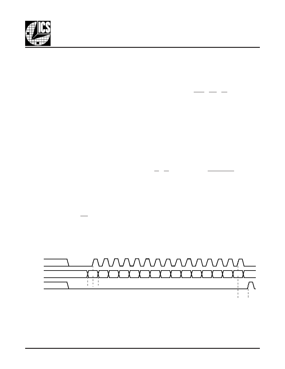
FIGURE 1. SERIAL LOAD OPERATIONS
t
S
t
H
t
S
S_CLOCK
S_DATA
S_LOAD
NOTE: Default Output Frequency, using a 16.66MHz crystal
on power-up = 200MHz (M = 192, N = 2) SSC off
T1
T0
N2
N1
N0
M8
M7
M6
M5
M4
M3
M2
M1
M0
SSC
(Power-up
Default)
相关PDF资料 |
PDF描述 |
|---|---|
| ICS8427BK-02LFT | 700 MHz, OTHER CLOCK GENERATOR, QCC32 |
| ICS8427BK-02T | 700 MHz, OTHER CLOCK GENERATOR, QCC32 |
| ICS8427DK-02T | 500 MHz, OTHER CLOCK GENERATOR, QCC32 |
| ICS843001AG-21T | 700 MHz, OTHER CLOCK GENERATOR, PDSO24 |
| ICS843001AG-21T | 700 MHz, OTHER CLOCK GENERATOR, PDSO24 |
相关代理商/技术参数 |
参数描述 |
|---|---|
| ICS8427DK-02 | 制造商:ICS 制造商全称:ICS 功能描述:500MHZ, LOW JITTER LVCMOS/CRYSTAL-TO-LVHSTL FREQUENCY SYNTHESIZER |
| ICS8427DK-02LF | 制造商:ICS 制造商全称:ICS 功能描述:500MHZ, LOW JITTER LVCMOS/CRYSTAL-TO-LVHSTL FREQUENCY SYNTHESIZER |
| ICS8427DK-02LFT | 制造商:ICS 制造商全称:ICS 功能描述:500MHZ, LOW JITTER LVCMOS/CRYSTAL-TO-LVHSTL FREQUENCY SYNTHESIZER |
| ICS8427DK-02T | 制造商:ICS 制造商全称:ICS 功能描述:500MHZ, LOW JITTER LVCMOS/CRYSTAL-TO-LVHSTL FREQUENCY SYNTHESIZER |
| ICS8427DY-02 | 制造商:ICS 制造商全称:ICS 功能描述:500MHZ, LOW JITTER LVCMOS/CRYSTAL-TO-LVHSTL FREQUENCY SYNTHESIZER |
发布紧急采购,3分钟左右您将得到回复。