- 您现在的位置:买卖IC网 > PDF目录1998 > ICS8430S10BYI-02LF (IDT, Integrated Device Technology Inc)IC CLK GENERATOR PLL 48TQFP PDF资料下载
参数资料
| 型号: | ICS8430S10BYI-02LF |
| 厂商: | IDT, Integrated Device Technology Inc |
| 文件页数: | 14/31页 |
| 文件大小: | 0K |
| 描述: | IC CLK GENERATOR PLL 48TQFP |
| 标准包装: | 250 |
| 类型: | 时钟/频率发生器,扇出缓冲器(分配),多路复用器 |
| PLL: | 是 |
| 主要目的: | Cavium 处理器 |
| 输入: | LVCMOS,LVDS,LVPECL,LVTTL,SSTL,晶体 |
| 输出: | LVCMOS,LVDS,LVPECL,LVTTL |
| 电路数: | 1 |
| 比率 - 输入:输出: | 2:10 |
| 差分 - 输入:输出: | 是/是 |
| 频率 - 最大: | 133.33MHz |
| 电源电压: | 3.135 V ~ 3.465 V |
| 工作温度: | -40°C ~ 85°C |
| 安装类型: | 表面贴装 |
| 封装/外壳: | 48-TQFP 裸露焊盘 |
| 供应商设备封装: | 48-PTQFP-EP(7x7) |
| 包装: | 托盘 |
第1页第2页第3页第4页第5页第6页第7页第8页第9页第10页第11页第12页第13页当前第14页第15页第16页第17页第18页第19页第20页第21页第22页第23页第24页第25页第26页第27页第28页第29页第30页第31页
ICS8430S10BYI-02 REVISION C JANUARY 17, 2011
21
2011 Integrated Device Technology, Inc.
ICS8430S10I-02 Data Sheet
CLOCK GENERATOR FOR CAVIUM PROCESSORS
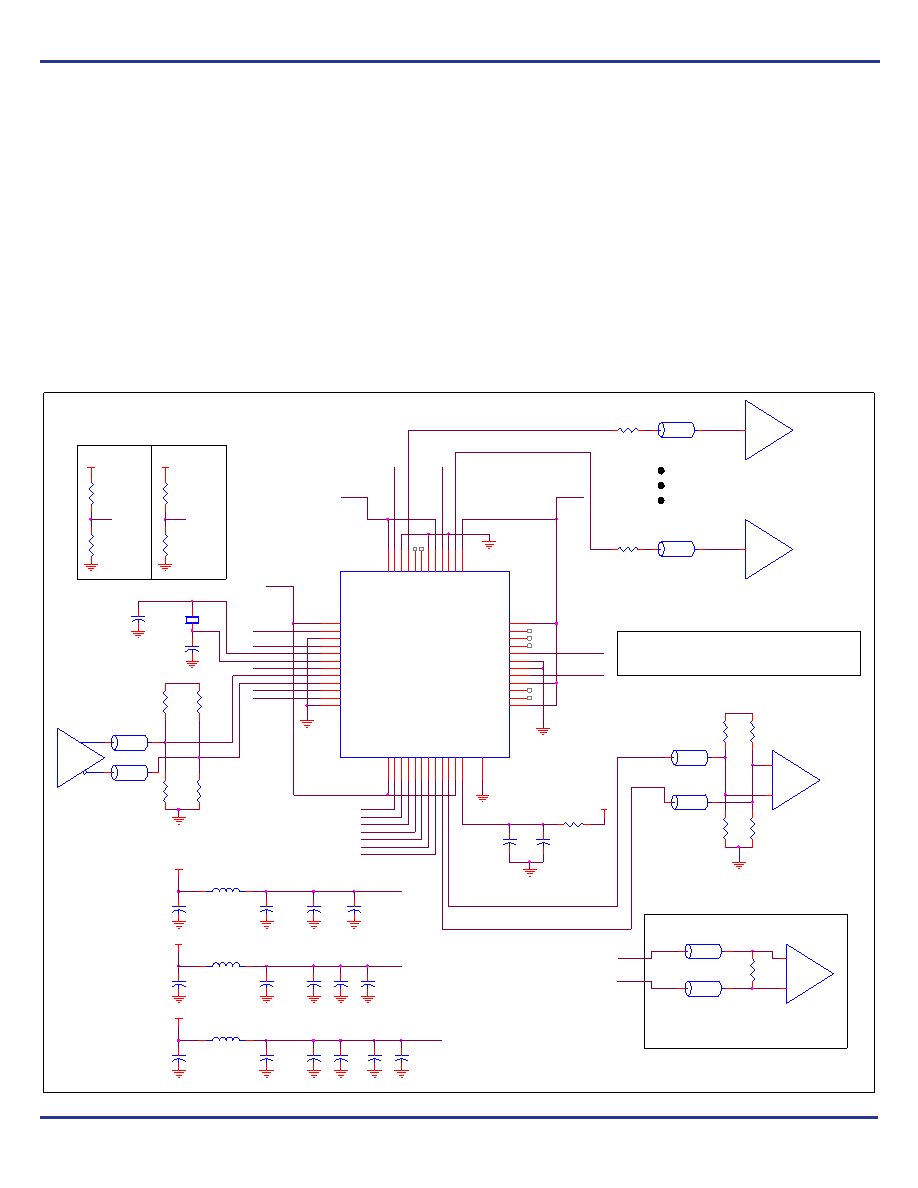
Schematic Example
Figure 7 shows an example of ICS8430S10I-02 application
schematic. In this example, the device is operated at VDD = VDDO_B
= VDDO_CD = VDDO_E = VDDO_REF = 3.3V. An 18pF parallel resonant
25MHz crystal is used. The load capacitance C1 = 18pF and C2 =
18pF are recommended for frequency accuracy. Depending on the
parasitics of the printed circuit board layout, these values might
require a slight adjustment to optimize the frequency accuracy.
Crystals with other load capacitance specifications can be used. This
will require adjusting C1 and C2. For this device, the crystal load
capacitors are required for proper operation.
As with any high speed analog circuitry, the power supply pins are
vulnerable to noise. To achieve optimum jitter performance, power
supply isolation is required. The ICS8430S10I-02 provides separate
power supplies to isolate from coupling into the internal PLL.
In order to achieve the best possible filtering, it is recommended that
the placement of the filter components be on the device side of the
PCB as close to the power pins as possible. If space is limited, the
0.1uF capacitor in each power pin filter should be placed on the
device side of the PCB and the other components can be placed on
the opposite side.
Power supply filter recommendations are a general guideline to be
used for reducing external noise from coupling into the devices. This
low-pass filter starts to attenuate noise at approximately 10kHz. If a
specific frequency noise component is known, such as switching
power supply frequencies, it is recommended that component values
be adjusted and if required, additional filtering be added. Additionally,
good general design practices for power plane voltage stability
suggests adding bulk capacitances in the local area of all devices.
The schematic example focuses on functional connections and is not
configuration specific. Refer to the pin description and functional
tables in the datasheet to ensure the logic control inputs are properly
set.
Figure 7. ICS8430S10I-02 Layout Example
RD1
Not Install
Zo = 50
To Logic
Input
pins
BLM18BB221SN2
Ferrite Bead
1
2
DDR_SEL0
3.3V
R2
33
nQA0
U1
37
38
39
40
41
42
43
44
45
46
47
48
1
2
4
3
5
6
7
8
9
10
11
12
24
23
22
21
20
19
18
17
16
15
14
13
36
35
34
33
32
31
30
29
28
27
26
25
49
V
DDO
_
E
QE
GN
D
LV
D
S
_
S
E
L
V
DDO
_RE
F
GN
D
QR
E
F
2
QR
E
F
1
QR
E
F
0
GN
D
nO
E
_E
V
DDO
_RE
F
VDD
nOE_D
nPLL_SEL
GND
XTAL_IN
XTAL_OUT
nXTAL_SEL
CLK
nCLK
nOE_C
nOE_B
GND
V
DDA
VD
D
QA
nQ
A
DDR_
S
E
L0
DDR_
S
E
L1
PC
I_
SE
L
0
PC
I_
SE
L
1
SPI
_
S
EL
0
SPI
_
S
EL
1
nO
E
_A
VD
D
VDDO_CD
QC
QD0
QD1
CORE_SEL
GND
nOE_REF
VDDO_B
QB0
QB1
VDDO_B
PAD
(U1:13)
VDD= VDDO_B = 3.3V
R12
100
QA0
X1
25MHz
+
-
VDDO_REF
nOE_D
VDD
nO
E
_E
C3
0.01u
RU2
Not Install
(U1:36)
VDD
VDDO
Zo = 50 Ohm
3.3V
DDR_SEL1
nQA0
C15
10uF
Set Logic
Input to
'0'
SPI_SEL0
R4
125
CLK
C13
0.1uF
C18
0.1uF
R3
125
Zo = 50 Ohm
VDD
R5
133
C9
0.1uF
VDDO_REF
(U1:37)
QA0
Zo = 50
SPI_SEL1
RU1
1K
VDDO
Zo = 50 Ohm
C11
0.1uF
VDDA
nOE_REF
C4
10u
XTAL_IN
Logic Control Input Examples
R1
33
To Logic
Input
pins
C19
0.1uF
C12
0.1uF
LVDS
Termination
Zo = 50 Ohm
C2
18pF
nOE_A
VDDO_REF
Set Logic
Input to
'1'
C16
0.1uF
C7
0.1uF
nXTAL_SEL
(U1:28)
PCI_SEL0
nCLK
BLM18BB221SN1
Ferrite Bead
1
2
nPLL_SEL
R6
133
nQA0
Zo = 50
VDD
CORE_SEL
C8
0.1uF
nOE_B
PCI_SEL1
R7
84
(U1:23)
C17
0.1uF
VDDO_CD = VDDO_E= VDDO_REF = 3.3V
RD2
1K
C6
10uF
+
-
C14
0.1uF
VDD
nOE_C
R8
84
(U1:41)
QA0
3.3V
QREF0
LVPECL
Termination
XTAL_OUT
C10
10uF
LVPECL Driv er
L
V
D
S_
SEL
R9
10
Receiv er
BLM18BB221SN3
Ferrite Bead
1
2
(U1:25)
3.3V
QE
(U1:48)
Zo = 50
Receiv er
VDD
R11
82.5
C5
0.1uF
VDDO
(U1:1)
VDD
R10
82.5
C1
18pF
1 8 p F
相关PDF资料 |
PDF描述 |
|---|---|
| ICS84314AY-02LFT | IC SYNTHESIZER 700MHZ 32-LQFP |
| ICS843156AKILF | IC CLK GENERATOR 32VFQFP |
| ICS843156AKLF | IC CLK GENERATOR 32VFQFP |
| ICS843202AYILF | IC SYNTHESIZER 680MHZ 32-LQFP |
| ICS843204AGILF | IC SYNTHESIZER LVPECL 48-TSSOP |
相关代理商/技术参数 |
参数描述 |
|---|---|
| ICS8430S10BYI-02LFT | 功能描述:IC CLK GENERATOR PLL 48TQFP RoHS:是 类别:集成电路 (IC) >> 时钟/计时 - 专用 系列:- 标准包装:1,500 系列:- 类型:时钟缓冲器/驱动器 PLL:是 主要目的:- 输入:- 输出:- 电路数:- 比率 - 输入:输出:- 差分 - 输入:输出:- 频率 - 最大:- 电源电压:3.3V 工作温度:0°C ~ 70°C 安装类型:表面贴装 封装/外壳:28-SSOP(0.209",5.30mm 宽) 供应商设备封装:28-SSOP 包装:带卷 (TR) 其它名称:93786AFT |
| ICS8430S10I-03 | 制造商:IDT 制造商全称:Integrated Device Technology 功能描述:Clock Generator for Cavium Processors |
| ICS8431-01 | 制造商:ICS 制造商全称:ICS 功能描述:200MHZ, LOW JITTER, LVPECL FREQUENCY SYNTHESIZER |
| ICS843101-312 | 制造商:ICS 制造商全称:ICS 功能描述:FEMTOCLOCKS⑩ CRYSTAL-TO-LVPECL 312.5MHZ FREQUENCY MARGINING SYNTHESIZER |
| ICS843101AG-312 | 制造商:ICS 制造商全称:ICS 功能描述:FEMTOCLOCKS⑩ CRYSTAL-TO-LVPECL 312.5MHZ FREQUENCY MARGINING SYNTHESIZER |
发布紧急采购,3分钟左右您将得到回复。