- 您现在的位置:买卖IC网 > PDF目录67690 > ICS8431CM-11LFT (INTEGRATED DEVICE TECHNOLOGY INC) 255 MHz, OTHER CLOCK GENERATOR, PDSO28 PDF资料下载
参数资料
| 型号: | ICS8431CM-11LFT |
| 厂商: | INTEGRATED DEVICE TECHNOLOGY INC |
| 元件分类: | 时钟产生/分配 |
| 英文描述: | 255 MHz, OTHER CLOCK GENERATOR, PDSO28 |
| 封装: | 7.50 X 18.05, 2.25 MM HEIGHT, SOIC-28 |
| 文件页数: | 4/18页 |
| 文件大小: | 2136K |
| 代理商: | ICS8431CM-11LFT |
8431CM-11
www.icst.com/products/hiperclocks.html
REV. B AUGUST 7, 2002
12
Integrated
Circuit
Systems, Inc.
ICS8431-11
255MHZ, LOW JITTER, CRYSTAL OSCILLATOR-
TO
-3.3V LVPECL FREQUENCY SYNTHESIZER
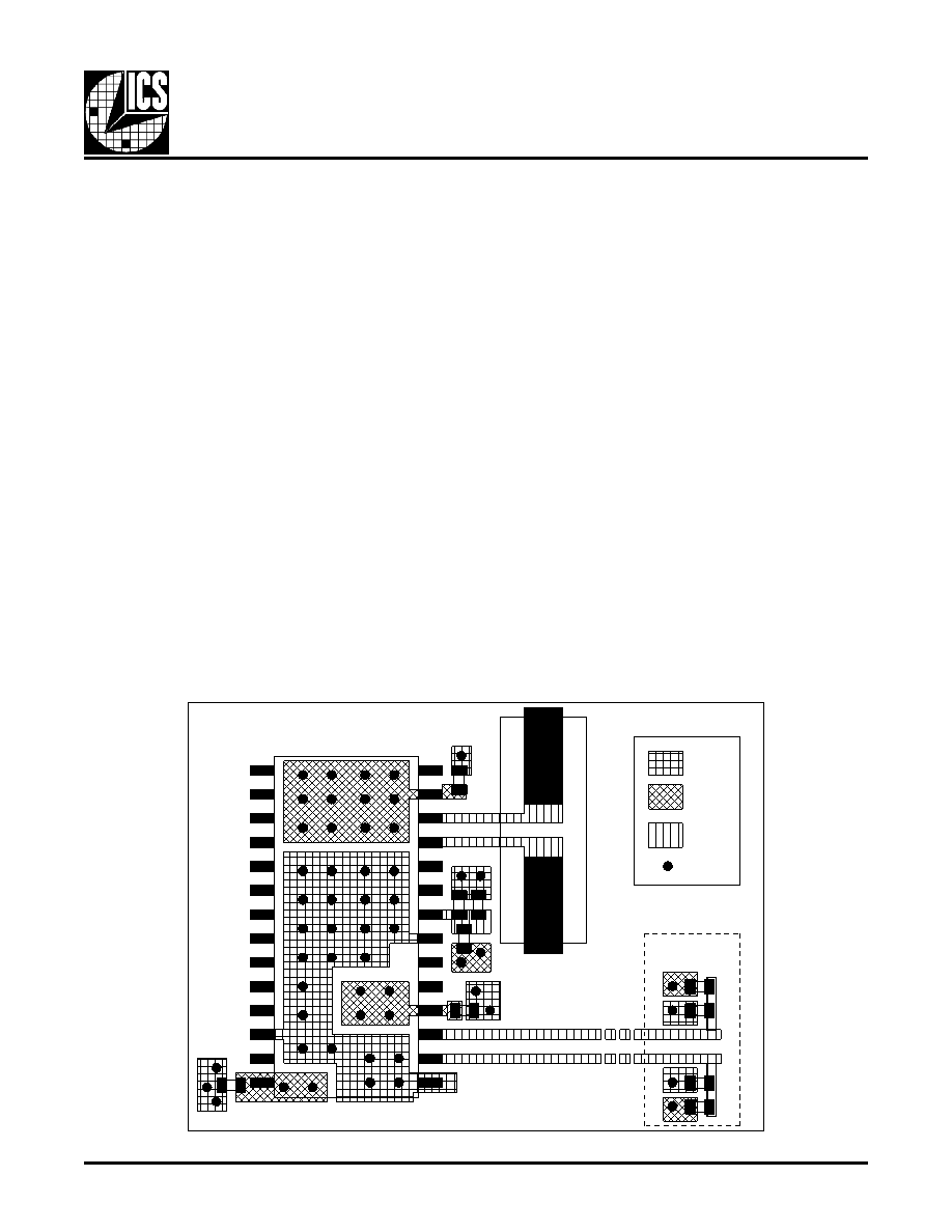
FIGURE 5B - PCB BOARD LAYOUT FOR ICS8431-11
R5
VIA
ICS8431-11
C4
IN+
TL1 (50 Ohm)
C6
IN-
R2
R4
R3
VCC
Close to the input
pins of the
receiver
X1
Signals
TL2 (50 Ohm)
R1
C3
C1
C2
GND
U1
The following component footprints are used in this layout
example:
All the resistors and capacitors are size 0603.
POWER AND GROUNDING
Place the decoupling capacitors C1, C2, C3, C4, and C6, as
close as possible to the power pins. If space allows, placment of
the decoupling capacitor on the component side is preferred. This
can reduce unwanted inductance between the decoupling ca-
pacitor and the power pin generated by the via.
Maximize the power and ground pad sizes and number of vias
capacitors. This can reduce the inductance between the power
and ground planes and the component power and ground pins.
The RC filter consisting of R5, C3, and C4 should be placed as
close to the V
CCA pin as possible.
CLOCK TRACES AND TERMINATION
Poor signal integrity can degrade the system performance or
cause system failure. In synchronous high-speed digital systems,
the clock signal is less tolerant to poor signal integrity than other
signals. Any ringing on the rising or falling edge or excessive ring
back can cause system failure. The shape of the trace and the
trace delay might be restricted by the available space on the board
and the component location. While routing the traces, the clock
signal traces should be routed first and should be locked prior to
routing other signal traces.
The differential 50
output traces should have same
length.
Avoid sharp angles on the clock trace. Sharp angle turns
cause the characteristic impedance to change on the
transmission lines.
Keep the clock traces on the same layer. Whenever pos-
sible, avoid placing vias on the clock traces. Placement
of vias on the traces can affect the trace characteristic
impedance and hence degrade signal integrity.
To prevent cross talk, avoid routing other signal traces in
parallel with the clock traces. If running parallel traces is
unavoidable, allow a separation of at least three trace
widths between the differential clock trace and the other
signal trace.
Make sure no other signal traces are routed between the
clock trace pair.
The matching termination resistors should be located as
close to the receiver input pins as possible.
The matching termination resistors R1, R2, R3 and R4 should
be located as close to the receiver input pins as possible.
Other termination scheme can also be used but is not shown
in the example.
CRYSTAL
The crystal X1 should be located as close as possible to the pins
25 (XTAL1) and 26 (XTAL2). The trace length between the X1
and U1 should be kept to a minimum to avoid unwanted parasitic
inductance and capacitance. Other signal traces should not be
routed near the crystal traces.
相关PDF资料 |
PDF描述 |
|---|---|
| ICS8431DMI-01 | 200 MHz, OTHER CLOCK GENERATOR, PDSO28 |
| ICS8431DMI-01LFT | 200 MHz, OTHER CLOCK GENERATOR, PDSO28 |
| ICS8431DMI-01 | 200 MHz, OTHER CLOCK GENERATOR, PDSO28 |
| ICS8431EM-01 | 200 MHz, OTHER CLOCK GENERATOR, PDSO28 |
| ICS8431EM-01LF | 200 MHz, OTHER CLOCK GENERATOR, PDSO28 |
相关代理商/技术参数 |
参数描述 |
|---|---|
| ICS8431CM-11T | 制造商:ICS 制造商全称:ICS 功能描述:255MHZ, LOW JITTER, LVPECL FREQUENCY SYNTHESIZER |
| ICS8431EM11 | 制造商:ICS 功能描述: |
| ICS8431I-21 | 制造商:ICS 制造商全称:ICS 功能描述:350MHZ, LOW JITTER, CRYSTAL OSCILLATOR-TO-3.3V LVPECL FREQUENCY SYNTHESIZER |
| ICS84320-01 | 制造商:IDT 制造商全称:Integrated Device Technology 功能描述:780MHZ, CRYSTAL-TO-3.3V DIFFERENTIAL LVPECL FREQUENCY SYNTHESIZER |
| ICS84320-01K | 制造商:ICS 制造商全称:ICS 功能描述:780MHZ, CRYSTAL-TO-3.3V DIFFERENTIAL LVPECL FREQUENCY SYNTHESIZER |
发布紧急采购,3分钟左右您将得到回复。