- 您现在的位置:买卖IC网 > PDF目录67691 > ICS843256AGLFT (INTEGRATED DEVICE TECHNOLOGY INC) 333.33 MHz, OTHER CLOCK GENERATOR, PDSO24 PDF资料下载
参数资料
| 型号: | ICS843256AGLFT |
| 厂商: | INTEGRATED DEVICE TECHNOLOGY INC |
| 元件分类: | 时钟产生/分配 |
| 英文描述: | 333.33 MHz, OTHER CLOCK GENERATOR, PDSO24 |
| 封装: | 4.40 X 7.80 MM, 0.92 MM HEIGHT, ROHS COMPLIANT, MO-153, TSSOP-24 |
| 文件页数: | 14/14页 |
| 文件大小: | 816K |
| 代理商: | ICS843256AGLFT |
IDT / ICS 3.3V LVPECL FREQUENCY SYNTHESIZER
9
ICS843256AM REV. A NOVEMBER 15, 2006
ICS843256
FEMTOCLOCKS CRYSTAL-TO-3.3V LVPECL FREQUENCY SYNTHESIZER
PRELIMINARY
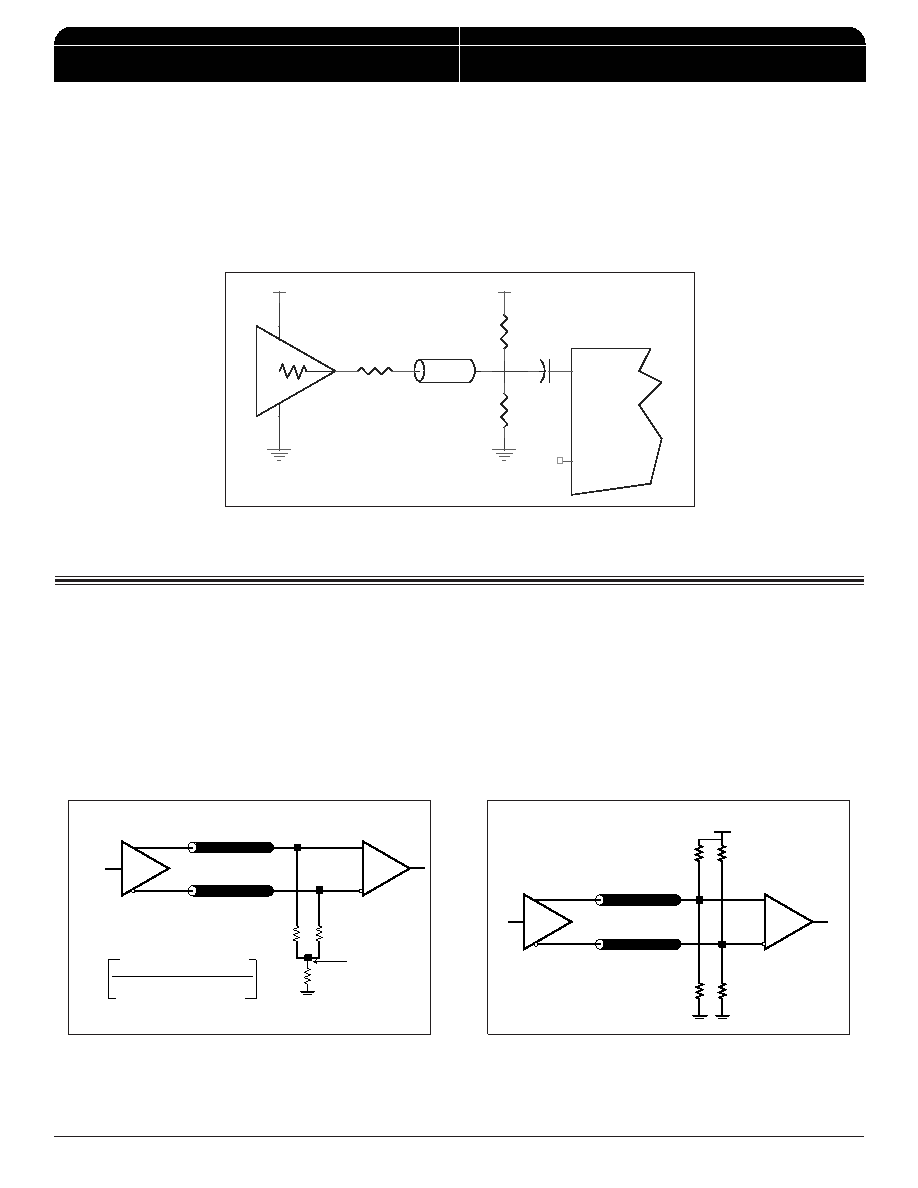
LVCMOS TO XTAL INTERFACE
The XTAL_IN input can accept a single-ended LVCMOS signal
through an AC coupling capacitor. A general interface diagram is
shown in
Figure 3 The XTAL_OUT pin can be left floating. The
input edge rate can be as slow as 10ns. For LVCMOS inputs, it is
recommended that the amplitude be reduced from full swing to
half swing in order to prevent signal interference with the power
rail and to reduce noise. This configuration requires that the output
FIGURE 3. GENERAL DIAGRAM FOR LVCMOS DRIVER TO XTAL INPUT INTERFACE
impedance of the driver (Ro) plus the series resistance (Rs) equals
the transmission line impedance. In addition, matched termination
at the crystal input will attenuate the signal in half. This can be
done in one of two ways. First, R1 and R2 in parallel should equal
the transmission line impedance. For most 50
applications, R1
and R2 can be 100
. This can also be accomplished by removing
R1 and making R2 50
.
R2
Zo = 50
VDD
Ro
Zo = Ro + Rs
R1
VDD
XTAL_IN
XTAL_OUT
.1uf
Rs
V
CC - 2V
50
50
RTT
Z
o = 50
Z
o = 50
FOUT
FIN
RTT =
Z
o
1
((V
OH + VOL) / (VCC – 2)) – 2
3.3V
125
125
84
84
Z
o = 50
Z
o = 50
FOUT
FIN
The clock layout topology shown below is a typical termination
for LVPECL outputs. The two different layouts mentioned are
recommended only as guidelines.
FOUT and nFOUT are low impedance follower outputs that gen-
erate ECL/LVPECL compatible outputs. Therefore, terminating
resistors (DC current path to ground) or current sources must be
used for functionality. These outputs are designed to drive 50
transmission lines. Matched impedance techniques should be
used to maximize operating frequency and minimize signal dis-
tortion.
Figures 4A and 4B show two different layouts which are
recommended only as guidelines. Other suitable clock layouts
may exist and it would be recommended that the board design-
ers simulate to guarantee compatibility across all printed circuit
and clock component process variations.
TERMINATION FOR LVPECL OUTPUTS
FIGURE 4B. LVPECL OUTPUT TERMINATION
FIGURE 4A. LVPECL OUTPUT TERMINATION
相关PDF资料 |
PDF描述 |
|---|---|
| ICS843256AM | 333.33 MHz, OTHER CLOCK GENERATOR, PDSO24 |
| ICS843256AG | 333.33 MHz, OTHER CLOCK GENERATOR, PDSO24 |
| ICS843256AMT | 333.33 MHz, OTHER CLOCK GENERATOR, PDSO24 |
| ICS843256BGI | 625 MHz, OTHER CLOCK GENERATOR, PDSO24 |
| ICS843256BGIT | 625 MHz, OTHER CLOCK GENERATOR, PDSO24 |
相关代理商/技术参数 |
参数描述 |
|---|---|
| ICS843256AGT | 制造商:ICS 制造商全称:ICS 功能描述:FEMTOCLOCKS⑩ CRYSTAL-TO-3.3V LVPECL FREQUENCY SYNTHESIZER W/INTEGRATED FANOUT BUFFER |
| ICS843256AM | 制造商:ICS 制造商全称:ICS 功能描述:FEMTOCLOCKS⑩ CRYSTAL-TO-3.3V LVPECL FREQUENCY SYNTHESIZER W/INTEGRATED FANOUT BUFFER |
| ICS843256AMLF | 制造商:ICS 制造商全称:ICS 功能描述:FEMTOCLOCKS⑩ CRYSTAL-TO-3.3V LVPECL FREQUENCY SYNTHESIZER W/INTEGRATED FANOUT BUFFER |
| ICS843256AMLFT | 制造商:ICS 制造商全称:ICS 功能描述:FEMTOCLOCKS⑩ CRYSTAL-TO-3.3V LVPECL FREQUENCY SYNTHESIZER W/INTEGRATED FANOUT BUFFER |
| ICS843256AMT | 制造商:ICS 制造商全称:ICS 功能描述:FEMTOCLOCKS⑩ CRYSTAL-TO-3.3V LVPECL FREQUENCY SYNTHESIZER W/INTEGRATED FANOUT BUFFER |
发布紧急采购,3分钟左右您将得到回复。