- 您现在的位置:买卖IC网 > PDF目录8992 > ICS84329BV-01LFT (IDT, Integrated Device Technology Inc)IC SYNTHESIZER 700MHZ 28-PLCC PDF资料下载
参数资料
| 型号: | ICS84329BV-01LFT |
| 厂商: | IDT, Integrated Device Technology Inc |
| 文件页数: | 12/21页 |
| 文件大小: | 0K |
| 描述: | IC SYNTHESIZER 700MHZ 28-PLCC |
| 标准包装: | 500 |
| 系列: | HiPerClockS™ |
| 类型: | 频率合成器 |
| PLL: | 是 |
| 输入: | 晶体 |
| 输出: | LVPECL |
| 电路数: | 1 |
| 比率 - 输入:输出: | 1:1 |
| 差分 - 输入:输出: | 无/是 |
| 频率 - 最大: | 700MHz |
| 除法器/乘法器: | 是/无 |
| 电源电压: | 3.135 V ~ 3.465 V |
| 工作温度: | 0°C ~ 70°C |
| 安装类型: | 表面贴装 |
| 封装/外壳: | 28-LCC(J 形引线) |
| 供应商设备封装: | 28-PLCC(11.5x11.5) |
| 包装: | 带卷 (TR) |
| 其它名称: | 84329BV-01LFT |
ICS84329B-01
700MHZ, LOW JITTER, CRYSTAL-TO-3.3V LVPECL FREQUENCY SYNTHESIZER
IDT / ICS LVPECL FREQUENCY SYNTHESIZER
2
ICS84329BM-01 REV. C AUGUST 19, 2013
Functional Description
NOTE: The functional description that follows describes operation
using a 16MHz crystal. Valid PLL loop divider values for different
crystal or input frequencies are defined in the Input Frequency
Characteristics, Table 6, NOTE 1.
The ICS84329B-01 features a fully integrated PLL and therefore
requires no external components for setting the loop bandwidth. A
parallel resonant, fundamental crystal is used as the input to the
on-chip oscillator. The output of the oscillator is divided by 16 prior
to the phase detector. With a 16MHz crystal this provides a 1MHz
reference frequency. The VCO of the PLL operates over a range
of 250MHz to 700MHz. The output of the M divider is also applied
to the phase detector.
The phase detector and the M divider force the VCO output
frequency to be M times the reference frequency ÷ 16 by adjusting
the VCO control voltage. Note that for some values of M (either too
high or too low), the PLL will not achieve lock. The output of the
VCO is scaled by a divider prior to being sent to each of the
LVPECL output buffers. The divider provides a 50% output duty
cycle.
The programmable features of the ICS84329B-01 support two
input modes to program the M divider and N output divider.
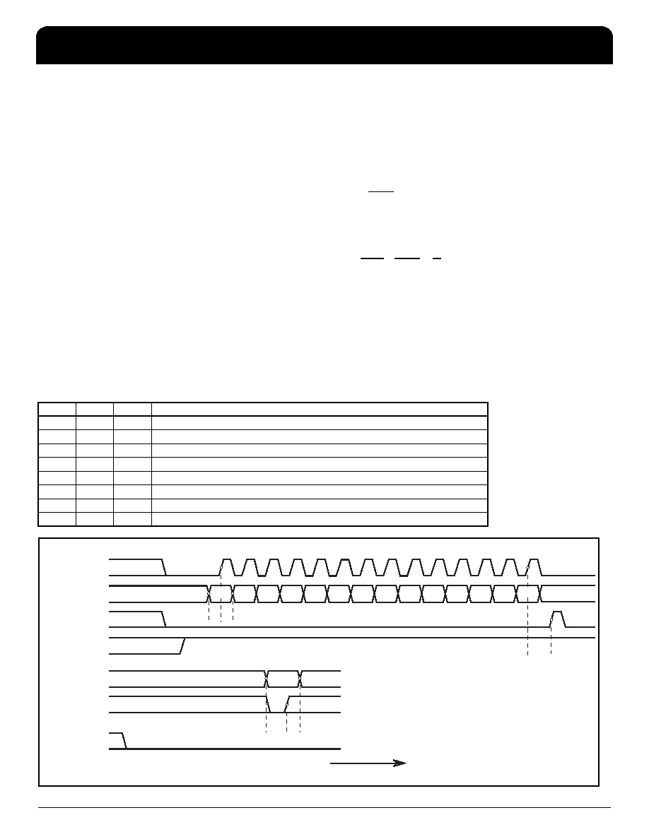
The two input operational modes are parallel and serial. Figure 1
shows the timing diagram for each mode. In parallel mode the
nP_LOAD input is LOW. The data on inputs M0 through M8 and N0
through N1 is passed directly to the M divider and N output divider.
On the LOW-to-HIGH transition of the nP_LOAD input, the data is
latched and the M divider remains loaded until the next LOW
transition on nP_LOAD or until a serial event occurs. The TEST
output is Mode 000 (shift register out) when operating in the
parallel input mode. The relationship between the VCO frequency,
the crystal frequency and the M divider is defined as follows:
fVCO = fXTAL x M
16
The M value and the required values of M0 through M8 are shown
in Table 3B, Programmable VCO Frequency Function Table. Valid
M values for which the PLL will achieve lock are defined as
250
M 511. The frequency out is defined as follows:
fout = fVCO = fXTAL x M
N16
N
Serial operation occurs when nP_LOAD is HIGH and S_LOAD is
LOW. The shift register is loaded by sampling the S_DATA bits with
the rising edge of S_CLOCK. The contents of the shift register are
loaded into the M divider when S_LOAD transitions from
LOW-to-HIGH. The M divide and N output divide values are
latched on the HIGH-to-LOW transition of S_LOAD. If S_LOAD is
held HIGH, data at the S_DATA input is passed directly to the M
divider on each rising edge of S_CLOCK. The serial mode can be
used to program the M and N bits and test bits T2:T0. The internal
resistors T2:T0 determine the state of the TEST output as follows:
T2
T1
T0
TEST Output
fOUT
0
Shift Register Out
fOUT
00
1
HIGH
fOUT
0
1
0
PLL Reference XTAL ÷16
fOUT
0
1
(VCO ÷ M) /2 (non 50% Duty Cycle M Divider)
fOUT
1
0
fOUT, LVCMOS Output Frequency < 200MHz
fOUT
10
1
LOW
fOUT
1
0
S_CLOCK ÷ M (non 50% Duty Cycle M Divider)
S_CLOCK ÷ N Divider
1
fOUT ÷ 4
fOUT
Time
SERIAL LOADING
PARALLEL LOADING
t
S
t
H
t
S
t
H
t
S
M, N
M0
M1
M2
M3
M4
M5
M6
M7
M8
N0
N1
T0
T1
T2
S_CLOCK
S_DATA
S_LOAD
nP_LOAD
M0:M8, N0:N1
nP_LOAD
Figure 1. Parallel & Serial Load Operations
相关PDF资料 |
PDF描述 |
|---|---|
| VI-20W-MY-F3 | CONVERTER MOD DC/DC 5.5V 50W |
| VI-20W-MY-F2 | CONVERTER MOD DC/DC 5.5V 50W |
| VI-2NP-MW-F3 | CONVERTER MOD DC/DC 13.8V 100W |
| AD5627RBRMZ-2 | IC DAC NANO 12BIT DUAL 10-MSOP |
| MS3454L20-14P | CONN RCPT 5POS JAM NUT W/PINS |
相关代理商/技术参数 |
参数描述 |
|---|---|
| ICS84329BV-01T | 制造商:Integrated Device Technology Inc 功能描述:IC SYNTHESIZER 700MHZ 28-PLCC |
| ICS84329BVLF | 功能描述:IC SYNTHESIZER 700MHZ 28-PLCC RoHS:是 类别:集成电路 (IC) >> 时钟/计时 - 时钟发生器,PLL,频率合成器 系列:HiPerClockS™ 标准包装:1,000 系列:- 类型:时钟/频率合成器,扇出分配 PLL:- 输入:- 输出:- 电路数:- 比率 - 输入:输出:- 差分 - 输入:输出:- 频率 - 最大:- 除法器/乘法器:- 电源电压:- 工作温度:- 安装类型:表面贴装 封装/外壳:56-VFQFN 裸露焊盘 供应商设备封装:56-VFQFP-EP(8x8) 包装:带卷 (TR) 其它名称:844S012AKI-01LFT |
| ICS84329BVLFT | 功能描述:IC SYNTHESIZER 700MHZ 28-PLCC RoHS:是 类别:集成电路 (IC) >> 时钟/计时 - 时钟发生器,PLL,频率合成器 系列:HiPerClockS™ 标准包装:1,000 系列:- 类型:时钟/频率合成器,扇出分配 PLL:- 输入:- 输出:- 电路数:- 比率 - 输入:输出:- 差分 - 输入:输出:- 频率 - 最大:- 除法器/乘法器:- 电源电压:- 工作温度:- 安装类型:表面贴装 封装/外壳:56-VFQFN 裸露焊盘 供应商设备封装:56-VFQFP-EP(8x8) 包装:带卷 (TR) 其它名称:844S012AKI-01LFT |
| ICS84329BVT | 制造商:ICS 制造商全称:ICS 功能描述:700MHZ, LOW JITTER, CRYSTAL-TO-3.3V DIFFERENTIAL LVPECL FREQUENCY SYNTHESIZER |
| ICS84329BY | 制造商:ICS 制造商全称:ICS 功能描述:700MHZ, LOW JITTER, CRYSTAL-TO-3.3V DIFFERENTIAL LVPECL FREQUENCY SYNTHESIZER |
发布紧急采购,3分钟左右您将得到回复。