- 您现在的位置:买卖IC网 > PDF目录67692 > ICS844101AGI-312LF 312.5 MHz, OTHER CLOCK GENERATOR, PDSO16 PDF资料下载
参数资料
| 型号: | ICS844101AGI-312LF |
| 元件分类: | 时钟产生/分配 |
| 英文描述: | 312.5 MHz, OTHER CLOCK GENERATOR, PDSO16 |
| 封装: | 4.40 X 5 MM, 0.92 MM HEIGHT, ROHS COMPLIANT, MO-153, TSSOP-16 |
| 文件页数: | 6/13页 |
| 文件大小: | 170K |
| 代理商: | ICS844101AGI-312LF |
844101AGI-312
www.icst.com/products/hiperclocks.html
REV. A NOVEMBER 28, 2005
2
Integrated
Circuit
Systems, Inc.
ICS844101I-312
FEMTOCLOCKS CRYSTAL-TO-LVDS
312.5MHZ FREQUENCY MARGINING SYNTHESIZER
PRELIMINARY
FUNCTIONAL DESCRIPTION
The ICS844101I-312 features a fully integrated PLL and
therefore requires no external components for setting the
loop bandwidth. A 25MHz fundamental crystal is used as
the input to the on chip oscillator. The output of the oscilla-
tor is fed into the pre-divider. In frequency margining mode,
the 25MHz crystal frequency is divided by 2 and a 12.5MHz
reference frequency is applied to the phase detector. The
VCO of the PLL operates over a range of 560MHz to
690MHz. The output of the M divider is also applied to the
phase detector.
The default mode for the ICS844101I-312 is 312.5MHz
output frequency using a 25MHz crystal. The output fre-
quency can be changed by placing the device into the
margining mode using the mode pin and using the serial
interface to program the M feedback divider. Frequency
margining mode operation occurs when the MODE input
is HIGH. The phase detector and the M divider force the
VCO output frequency to be M times the reference fre-
quency by adjusting the VCO control voltage. Note that for
some values of M (either too high or too low), the PLL will
not achieve lock. The output of the VCO is scaled by an
output divider prior to being sent to the LVPECL output
buffer. The divider provides a 50% output duty cycle. The
relationship between the crystal input frequency, the M
divider, the VCO frequency and the output frequency is
provided in Table 1. When changing back from frequency
margining mode to nominal mode, the device will return to
the default nominal configuration that will provide
312.5MHz output frequency.
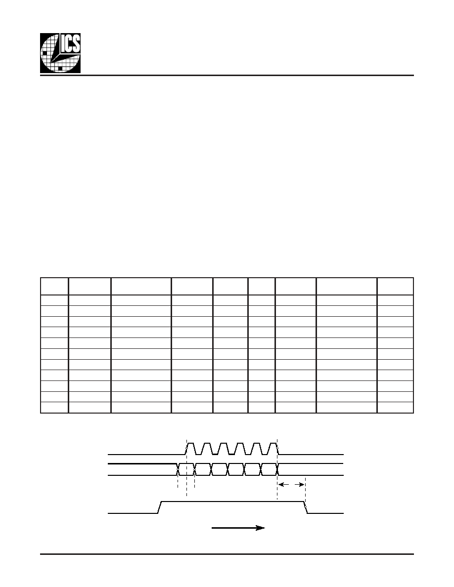
Serial operation occurs when S_LOAD is HIGH. Serial data
can be loaded in either the default mode or the frequency
margining mode. The 6-bit shift register is loaded by sam-
pling the S_DATA bits with the rising edge of S_CLOCK.
After shifting in the 6-bit M divider value, S_LOAD is
transitioned from HIGH to LOW which latches the contents of
the shift-register into the M divider control register. When
S_LOAD is LOW, any transitions of S_CLOCK or S_DATA
are ignored.
L
A
T
X
)
z
H
M
(
r
e
d
i
v
i
D
-
e
r
P
)
P
(
e
c
n
e
r
e
f
e
R
)
z
H
M
(
y
c
n
e
u
q
e
r
F
k
c
a
b
d
e
F
)
M
(
r
e
d
i
v
i
D
a
t
a
D
-
M
)
y
r
a
n
i
B
(
O
C
V
)
z
H
M
(
t
u
p
t
u
O
)
N
(
r
e
d
i
v
i
D
t
u
p
t
u
O
)
z
H
M
(
y
c
n
e
u
q
e
r
F
%
e
g
n
a
h
C
5
22
5
.
2
15
41
0
1
0
15
.
2
6
52
5
2
.
1
8
20
.
0
1
-
5
22
5
.
2
16
40
1
0
15
7
52
5
.
7
8
20
.
8
-
5
22
5
.
2
17
41
1
0
15
.
7
8
52
5
7
.
3
9
20
.
6
-
5
22
5
.
2
18
40
0
1
10
0
62
0
30
.
4
-
5
22
5
.
2
19
41
0
1
15
.
2
1
62
5
2
.
6
0
30
.
2
-
5
22
5
.
2
10
50
1
0
1
15
2
62
5
.
2
1
30
5
22
5
.
2
11
51
1
0
1
15
.
7
3
62
5
7
.
8
1
30
.
2
5
22
5
.
2
12
50
0
1
0
1
10
5
62
5
2
30
.
4
5
22
5
.
2
13
51
0
1
0
1
15
.
2
6
62
5
2
.
1
3
30
.
6
5
22
5
.
2
14
50
1
0
1
15
7
62
5
.
7
3
30
.
8
5
22
5
.
2
15
51
1
0
1
15
.
7
8
62
5
7
.
3
4
30
.
0
1
TABLE 1. FREQUENCY MARGIN FUNCTION TABLE
FIGURE 1. SERIAL LOAD OPERATIONS
Time
SERIAL LOADING
t
S
t
H
M5
M4
M3
M2
M1
M0
t
S
S_CLOCK
S_DATA
S_LOAD
相关PDF资料 |
PDF描述 |
|---|---|
| ICS844101AGI-312 | 312.5 MHz, OTHER CLOCK GENERATOR, PDSO16 |
| ICS844101AGI-312 | 312.5 MHz, OTHER CLOCK GENERATOR, PDSO16 |
| ICS844101AGI-312LFT | 312.5 MHz, OTHER CLOCK GENERATOR, PDSO16 |
| ICS844101AGI-312T | 312.5 MHz, OTHER CLOCK GENERATOR, PDSO16 |
| ICS844204BK-245T | OTHER CLOCK GENERATOR, QCC32 |
相关代理商/技术参数 |
参数描述 |
|---|---|
| ICS844201BG-45LF | 功能描述:IC CLK GENERATOR 25MHZ 8TSSOP RoHS:是 类别:集成电路 (IC) >> 时钟/计时 - 专用 系列:HiPerClockS™, FemtoClock™, PCI Express® (PCIe) 标准包装:1,500 系列:- 类型:时钟缓冲器/驱动器 PLL:是 主要目的:- 输入:- 输出:- 电路数:- 比率 - 输入:输出:- 差分 - 输入:输出:- 频率 - 最大:- 电源电压:3.3V 工作温度:0°C ~ 70°C 安装类型:表面贴装 封装/外壳:28-SSOP(0.209",5.30mm 宽) 供应商设备封装:28-SSOP 包装:带卷 (TR) 其它名称:93786AFT |
| ICS844201BG-45LFT | 功能描述:IC CLK GENERATOR 25MHZ 8TSSOP RoHS:是 类别:集成电路 (IC) >> 时钟/计时 - 专用 系列:HiPerClockS™, FemtoClock™, PCI Express® (PCIe) 标准包装:1,500 系列:- 类型:时钟缓冲器/驱动器 PLL:是 主要目的:- 输入:- 输出:- 电路数:- 比率 - 输入:输出:- 差分 - 输入:输出:- 频率 - 最大:- 电源电压:3.3V 工作温度:0°C ~ 70°C 安装类型:表面贴装 封装/外壳:28-SSOP(0.209",5.30mm 宽) 供应商设备封装:28-SSOP 包装:带卷 (TR) 其它名称:93786AFT |
| ICS844201BGI-45LF | 功能描述:IC CLK GENERATOR 25MHZ 8TSSOP RoHS:是 类别:集成电路 (IC) >> 时钟/计时 - 专用 系列:HiPerClockS™, FemtoClock™, PCI Express® (PCIe) 标准包装:1,500 系列:- 类型:时钟缓冲器/驱动器 PLL:是 主要目的:- 输入:- 输出:- 电路数:- 比率 - 输入:输出:- 差分 - 输入:输出:- 频率 - 最大:- 电源电压:3.3V 工作温度:0°C ~ 70°C 安装类型:表面贴装 封装/外壳:28-SSOP(0.209",5.30mm 宽) 供应商设备封装:28-SSOP 包装:带卷 (TR) 其它名称:93786AFT |
| ICS844201BGI-45LFT | 功能描述:IC CLK GENERATOR 25MHZ 8TSSOP RoHS:是 类别:集成电路 (IC) >> 时钟/计时 - 专用 系列:HiPerClockS™, FemtoClock™, PCI Express® (PCIe) 标准包装:1,500 系列:- 类型:时钟缓冲器/驱动器 PLL:是 主要目的:- 输入:- 输出:- 电路数:- 比率 - 输入:输出:- 差分 - 输入:输出:- 频率 - 最大:- 电源电压:3.3V 工作温度:0°C ~ 70°C 安装类型:表面贴装 封装/外壳:28-SSOP(0.209",5.30mm 宽) 供应商设备封装:28-SSOP 包装:带卷 (TR) 其它名称:93786AFT |
| ICS844202AK-245LF | 功能描述:IC CLOCK GEN SRL SCSI 32-VFQFPN RoHS:是 类别:集成电路 (IC) >> 时钟/计时 - 专用 系列:HiPerClockS™, PCI Express® (PCIe) 标准包装:28 系列:- 类型:时钟/频率发生器 PLL:是 主要目的:Intel CPU 服务器 输入:时钟 输出:LVCMOS 电路数:1 比率 - 输入:输出:3:22 差分 - 输入:输出:无/是 频率 - 最大:400MHz 电源电压:3.135 V ~ 3.465 V 工作温度:0°C ~ 85°C 安装类型:表面贴装 封装/外壳:64-TFSOP (0.240",6.10mm 宽) 供应商设备封装:64-TSSOP 包装:管件 |
发布紧急采购,3分钟左右您将得到回复。