- 您现在的位置:买卖IC网 > PDF目录67695 > ICS853013AMLF 853013 SERIES, LOW SKEW CLOCK DRIVER, 3 TRUE OUTPUT(S), 0 INVERTED OUTPUT(S), PDSO20 PDF资料下载
参数资料
| 型号: | ICS853013AMLF |
| 元件分类: | 时钟及定时 |
| 英文描述: | 853013 SERIES, LOW SKEW CLOCK DRIVER, 3 TRUE OUTPUT(S), 0 INVERTED OUTPUT(S), PDSO20 |
| 封装: | 7.50 X 12.80 MM, 2.30 MM HEIGHT, LEAD FREE, MS-013, MO-119, SOIC-20 |
| 文件页数: | 14/17页 |
| 文件大小: | 448K |
| 代理商: | ICS853013AMLF |
853013AM
www.icst.com/products/hiperclocks.html
REV. A OCTOBER 19, 2005
6
Integrated
Circuit
Systems, Inc.
ICS853013
LOW SKEW, DUAL, 1-TO-3, DIFFERENTIAL-TO-
2.5V/3.3V/5V LVPECL/ECL FANOUT BUFFER
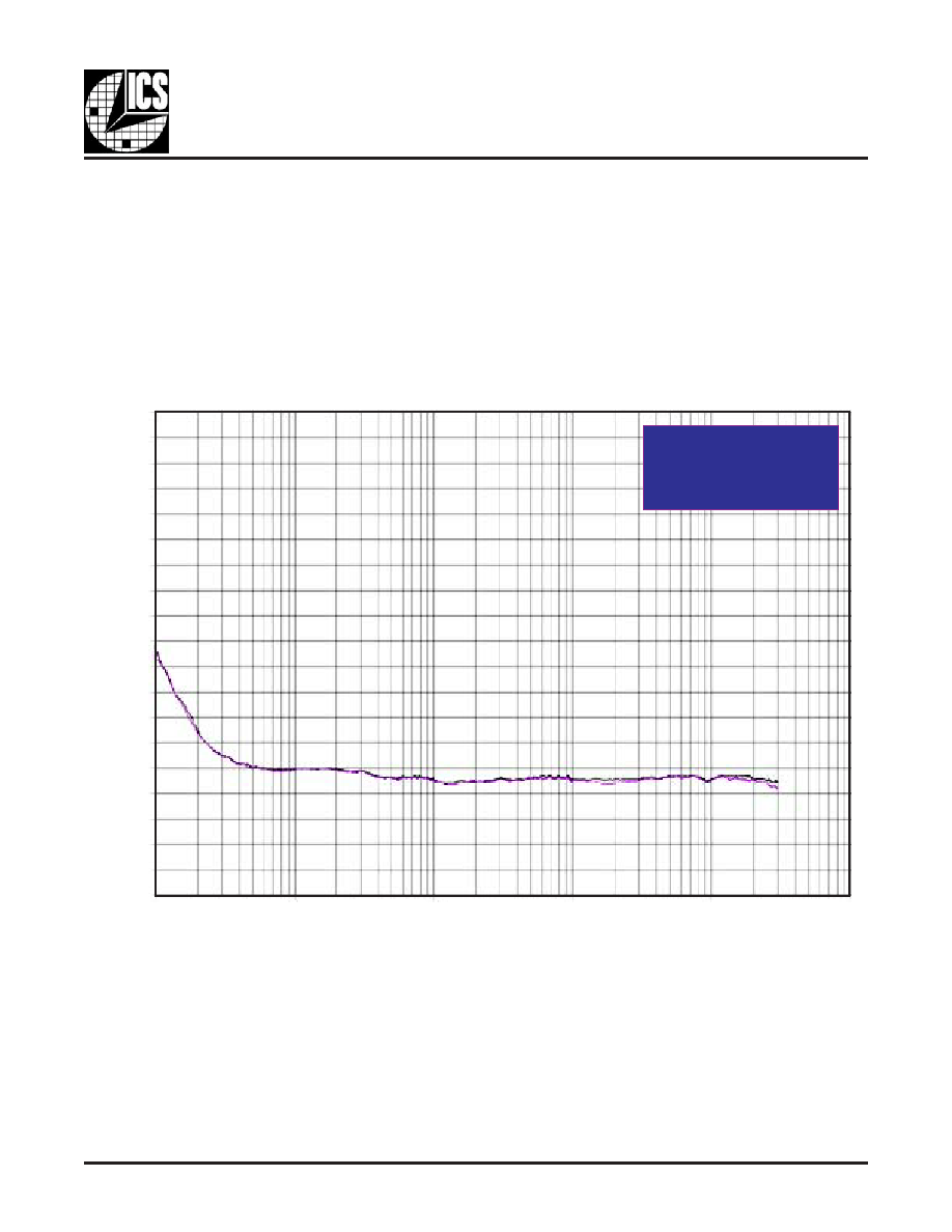
ADDITIVE PHASE JITTER
Input/Output Additive
Phase Jitter at 156.25MHz
= 0.03ps (typical)
0
-10
-20
-30
-40
-50
-60
-70
-80
-90
-100
-110
-120
-130
-140
-150
-160
-170
-180
-190
1k
10k
100k
1M
10M
100M
The spectral purity in a band at a specific offset from the funda-
mental compared to the power of the fundamental is called the
dBc Phase Noise. This value is normally expressed using a
Phase noise plot and is most often the specified plot in many
applications. Phase noise is defined as the ratio of the noise
power present in a 1Hz band at a specified offset from the fun-
damental frequency to the power value of the fundamental. This
ratio is expressed in decibels (dBm) or a ratio of the power in
As with most timing specifications, phase noise measurements
have issues. The primary issue relates to the limitations of the
equipment. Often the noise floor of the equipment is higher than
the noise floor of the device. This is illustrated above. The de-
the 1Hz band to the power in the fundamental. When the re-
quired offset is specified, the phase noise is called a dBc value,
which simply means dBm at a specified offset from the funda-
mental. By investigating jitter in the frequency domain, we get a
better understanding of its effects on the desired application over
the entire time record of the signal. It is mathematically possible
to calculate an expected bit error rate given a phase noise plot.
vice meets the noise floor of what is shown, but can actually be
lower. The phase noise is dependant on the input source and
measurement equipment.
OFFSET FROM CARRIER FREQUENCY (HZ)
SSB
P
HASE
N
OISE
dBc/H
Z
相关PDF资料 |
PDF描述 |
|---|---|
| ICS853013AMLFT | 853013 SERIES, LOW SKEW CLOCK DRIVER, 3 TRUE OUTPUT(S), 0 INVERTED OUTPUT(S), PDSO20 |
| ICS853013AMT | 853013 SERIES, LOW SKEW CLOCK DRIVER, 3 TRUE OUTPUT(S), 0 INVERTED OUTPUT(S), PDSO20 |
| ICS853014AG | LOW SKEW CLOCK DRIVER, 5 TRUE OUTPUT(S), 0 INVERTED OUTPUT(S), PDSO20 |
| ICS853014AGLF | LOW SKEW CLOCK DRIVER, 5 TRUE OUTPUT(S), 0 INVERTED OUTPUT(S), PDSO20 |
| ICS853014BGLFT | 853014 SERIES, LOW SKEW CLOCK DRIVER, 5 TRUE OUTPUT(S), 0 INVERTED OUTPUT(S), PDSO20 |
相关代理商/技术参数 |
参数描述 |
|---|---|
| ICS853013AMLFT | 功能描述:IC CLK BUFFER 1:3 2GHZ 20-TSSOP RoHS:是 类别:集成电路 (IC) >> 时钟/计时 - 时钟缓冲器,驱动器 系列:HiPerClockS™ 标准包装:1 系列:HiPerClockS™ 类型:扇出缓冲器(分配),多路复用器 电路数:1 比率 - 输入:输出:2:18 差分 - 输入:输出:是/无 输入:CML,LVCMOS,LVPECL,LVTTL,SSTL 输出:LVCMOS,LVTTL 频率 - 最大:250MHz 电源电压:2.375 V ~ 3.465 V 工作温度:0°C ~ 70°C 安装类型:表面贴装 封装/外壳:32-LQFP 供应商设备封装:32-TQFP(7x7) 包装:- 其它名称:800-1923-6 |
| ICS853014BGLF | 功能描述:IC CLOCK BUFFER MUX 2:5 20-TSSOP RoHS:是 类别:集成电路 (IC) >> 时钟/计时 - 时钟缓冲器,驱动器 系列:HiPerClockS™ 标准包装:1 系列:HiPerClockS™ 类型:扇出缓冲器(分配),多路复用器 电路数:1 比率 - 输入:输出:2:18 差分 - 输入:输出:是/无 输入:CML,LVCMOS,LVPECL,LVTTL,SSTL 输出:LVCMOS,LVTTL 频率 - 最大:250MHz 电源电压:2.375 V ~ 3.465 V 工作温度:0°C ~ 70°C 安装类型:表面贴装 封装/外壳:32-LQFP 供应商设备封装:32-TQFP(7x7) 包装:- 其它名称:800-1923-6 |
| ICS853014BGLFT | 功能描述:IC CLOCK BUFFER MUX 2:5 20-TSSOP RoHS:是 类别:集成电路 (IC) >> 时钟/计时 - 时钟缓冲器,驱动器 系列:HiPerClockS™ 标准包装:1 系列:HiPerClockS™ 类型:扇出缓冲器(分配),多路复用器 电路数:1 比率 - 输入:输出:2:18 差分 - 输入:输出:是/无 输入:CML,LVCMOS,LVPECL,LVTTL,SSTL 输出:LVCMOS,LVTTL 频率 - 最大:250MHz 电源电压:2.375 V ~ 3.465 V 工作温度:0°C ~ 70°C 安装类型:表面贴装 封装/外壳:32-LQFP 供应商设备封装:32-TQFP(7x7) 包装:- 其它名称:800-1923-6 |
| ICS853014BGT | 制造商:INT_CIR_SYS 功能描述: |
| ICS853016AGLF | 功能描述:IC CLOCK BUFFER 1:2 3GHZ 8-TSSOP RoHS:是 类别:集成电路 (IC) >> 时钟/计时 - 时钟缓冲器,驱动器 系列:HiPerClockS™ 标准包装:1 系列:HiPerClockS™ 类型:扇出缓冲器(分配),多路复用器 电路数:1 比率 - 输入:输出:2:18 差分 - 输入:输出:是/无 输入:CML,LVCMOS,LVPECL,LVTTL,SSTL 输出:LVCMOS,LVTTL 频率 - 最大:250MHz 电源电压:2.375 V ~ 3.465 V 工作温度:0°C ~ 70°C 安装类型:表面贴装 封装/外壳:32-LQFP 供应商设备封装:32-TQFP(7x7) 包装:- 其它名称:800-1923-6 |
发布紧急采购,3分钟左右您将得到回复。