- 您现在的位置:买卖IC网 > PDF目录8741 > ICS8545BGLF (IDT, Integrated Device Technology Inc)IC CLOCK BUFFER MUX 2:4 20-TSSOP PDF资料下载
参数资料
| 型号: | ICS8545BGLF |
| 厂商: | IDT, Integrated Device Technology Inc |
| 文件页数: | 8/10页 |
| 文件大小: | 0K |
| 描述: | IC CLOCK BUFFER MUX 2:4 20-TSSOP |
| 标准包装: | 74 |
| 系列: | HiPerClockS™ |
| 类型: | 扇出缓冲器(分配),多路复用器 |
| 电路数: | 1 |
| 比率 - 输入:输出: | 2:4 |
| 差分 - 输入:输出: | 无/是 |
| 输入: | LVCMOS,LVTTL |
| 输出: | LVDS |
| 频率 - 最大: | 650MHz |
| 电源电压: | 3.135 V ~ 3.465 V |
| 工作温度: | 0°C ~ 70°C |
| 安装类型: | 表面贴装 |
| 封装/外壳: | 20-TSSOP(0.173",4.40mm 宽) |
| 供应商设备封装: | 20-TSSOP |
| 包装: | 管件 |
| 其它名称: | 8545BGLF ICS8545BGLF-ND |
2006 Fairchild Semiconductor Corporation
www.fairchildsemi.com
FMS6203 Rev. 1.0.4
6
FM
S6203
—
Low-
C
ost
,3-
C
h
annel,
Video
Filt
er
D
river
f
o
rSD
/PS/H
D
Layout Considerations
General layout and supply bypassing play a major role
in
high-frequency
performance
and
thermal
characteristics. Fairchild offers an evaluation board to
guide layout and aid device evaluation. The evaluation
board is a four-layer board with full power and ground
planes. Following this layout configuration provides
optimum performance and thermal characteristics for
the device. For the best results, follow the steps and
recommended routing rules listed below.
Recommended Routing / Layout Rules
Do not run analog and digital signals in parallel.
Use separate analog and digital power planes to
supply power.
Run traces on top of the ground plane at all times.
Do not run traces over ground/power splits.
Avoid routing at 90-degree angles.
Minimize clock and video data trace length
differences.
Include 10F and 0.1F ceramic power supply
bypass capacitors.
Place the 0.1F capacitor within 0.1 inches of the
device power pin.
Place the 10F capacitor within 0.75 inches of the
device power pin.
For multi-layer boards, use a large ground plane to
help dissipate heat.
For two-layer boards, use a ground plane that
extends beyond the device body by at least 0.5
inches on all sides. Include a metal paddle under
the device on the top layer.
Minimize all trace lengths to reduce series
inductance.
Thermal Considerations
Since the interior of most systems, such as set-top
boxes, TVs, and DVD players, are at +70C;
consideration must be given to providing an adequate
heat sink for the device package for maximum heat
dissipation. When designing a system board, determine
how much power each device dissipates. Ensure that
devices of high power are not placed in the same
location, such as directly above (top plane) and below
bottom plane) each other on the PCB.
PCB Thermal Layout Considerations
Understand the system power requirements and
environmental conditions.
Maximize thermal performance of the PCB.
Consider 70m copper for high-power designs.
Make the PCB as thin as possible by reducing FR4
thickness.
Use vias in the power pad to tie adjacent layers
together.
Remember that baseline temperature is a function
of board area, not copper thickness.
Use modeling techniques for first-order
approximation.
Output Considerations
The FMS6203 outputs are DC offset from the input by
150mV; therefore, VOUT = 2VIN DC+150mV. This offset
is required to obtain optimal performance from the
output driver and is held at the minimum value to
decrease the standing DC current into the load. Since
the FMS6203 has a 2x (6dB) gain, the output is typically
connected via a 75-series back-matching resistor
followed by the 75 video cable. Because of the
inherent divide by two of this configuration, the blanking
level at the load of the video signal is always less than
1V. When AC-coupling the output, ensure that the
coupling capacitor of choice passes the lowest
frequency content in the video signal and that line time
distortion (video tilt) is kept as low as possible.
The selection of the coupling capacitor is a function of
the subsequent circuit input impedance and the leakage
current of the input being driven. To obtain the highest
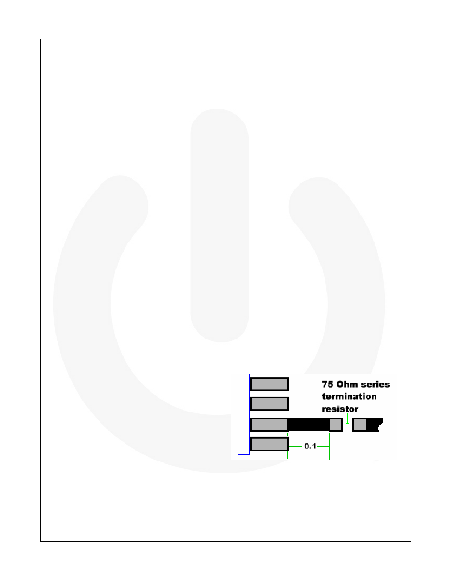
quality output video signal, the series termination
resistor must be placed as close to the device output
pin as possible. This greatly reduces the parasitic
capacitance and inductance effect on the FMS6203
output driver. Recommended distance from device pin
to place series termination resistor is no greater than
0.1 inches.
Figure 3.
Distance from Device Pin to Series
Termination Resistor
相关PDF资料 |
PDF描述 |
|---|---|
| VI-24V-MW-F1 | CONVERTER MOD DC/DC 5.8V 100W |
| VI-240-MW-F4 | CONVERTER MOD DC/DC 5V 100W |
| VI-240-MW-F3 | CONVERTER MOD DC/DC 5V 100W |
| VI-240-MW-F2 | CONVERTER MOD DC/DC 5V 100W |
| ICS8304AM-01LF | IC CLK BUFFER 1:4 166MHZ 8-SOIC |
相关代理商/技术参数 |
参数描述 |
|---|---|
| ICS8545BGLFT | 功能描述:IC CLOCK BUFFER MUX 2:4 20-TSSOP RoHS:是 类别:集成电路 (IC) >> 时钟/计时 - 时钟缓冲器,驱动器 系列:HiPerClockS™ 标准包装:74 系列:- 类型:扇出缓冲器(分配) 电路数:1 比率 - 输入:输出:1:10 差分 - 输入:输出:是/是 输入:HCSL, LVCMOS, LVDS, LVPECL, LVTTL 输出:HCSL,LVDS 频率 - 最大:400MHz 电源电压:3 V ~ 3.6 V 工作温度:-40°C ~ 85°C 安装类型:表面贴装 封装/外壳:32-VFQFN 裸露焊盘 供应商设备封装:32-QFN(5x5) 包装:管件 |
| ICS8546AG-01LF | 功能描述:IC CLOCK BUFFER MUX 3:6 24-TSSOP RoHS:是 类别:集成电路 (IC) >> 时钟/计时 - 时钟缓冲器,驱动器 系列:HiPerClockS™ 产品培训模块:High Bandwidth Product Overview 标准包装:1,000 系列:Precision Edge® 类型:扇出缓冲器(分配) 电路数:1 比率 - 输入:输出:1:4 差分 - 输入:输出:是/是 输入:CML,LVDS,LVPECL 输出:CML 频率 - 最大:2.5GHz 电源电压:2.375 V ~ 2.625 V 工作温度:-40°C ~ 85°C 安装类型:表面贴装 封装/外壳:16-VFQFN 裸露焊盘,16-MLF? 供应商设备封装:16-MLF?(3x3) 包装:带卷 (TR) |
| ICS8546AG-01LFT | 功能描述:IC CLOCK BUFFER MUX 3:6 24-TSSOP RoHS:是 类别:集成电路 (IC) >> 时钟/计时 - 时钟缓冲器,驱动器 系列:HiPerClockS™ 标准包装:74 系列:- 类型:扇出缓冲器(分配) 电路数:1 比率 - 输入:输出:1:10 差分 - 输入:输出:是/是 输入:HCSL, LVCMOS, LVDS, LVPECL, LVTTL 输出:HCSL,LVDS 频率 - 最大:400MHz 电源电压:3 V ~ 3.6 V 工作温度:-40°C ~ 85°C 安装类型:表面贴装 封装/外壳:32-VFQFN 裸露焊盘 供应商设备封装:32-QFN(5x5) 包装:管件 |
| ICS8547AY | 功能描述:IC CLK BUFFER 1:2 700MHZ 48-LQFP RoHS:否 类别:集成电路 (IC) >> 时钟/计时 - 时钟缓冲器,驱动器 系列:HiPerClockS™ 标准包装:74 系列:- 类型:扇出缓冲器(分配) 电路数:1 比率 - 输入:输出:1:10 差分 - 输入:输出:是/是 输入:HCSL, LVCMOS, LVDS, LVPECL, LVTTL 输出:HCSL,LVDS 频率 - 最大:400MHz 电源电压:3 V ~ 3.6 V 工作温度:-40°C ~ 85°C 安装类型:表面贴装 封装/外壳:32-VFQFN 裸露焊盘 供应商设备封装:32-QFN(5x5) 包装:管件 |
| ICS854S006AGILF | 功能描述:IC CLK BUFFER 1:6 1.7GHZ 24TSSOP RoHS:是 类别:集成电路 (IC) >> 时钟/计时 - 时钟缓冲器,驱动器 系列:HiPerClockS™ 标准包装:74 系列:- 类型:扇出缓冲器(分配) 电路数:1 比率 - 输入:输出:1:10 差分 - 输入:输出:是/是 输入:HCSL, LVCMOS, LVDS, LVPECL, LVTTL 输出:HCSL,LVDS 频率 - 最大:400MHz 电源电压:3 V ~ 3.6 V 工作温度:-40°C ~ 85°C 安装类型:表面贴装 封装/外壳:32-VFQFN 裸露焊盘 供应商设备封装:32-QFN(5x5) 包装:管件 |
发布紧急采购,3分钟左右您将得到回复。