- 您现在的位置:买卖IC网 > PDF目录9147 > ICS87004AGLF (IDT, Integrated Device Technology Inc)IC CLK GENERATOR ZD 1:4 24-TSSOP PDF资料下载
参数资料
| 型号: | ICS87004AGLF |
| 厂商: | IDT, Integrated Device Technology Inc |
| 文件页数: | 2/15页 |
| 文件大小: | 0K |
| 描述: | IC CLK GENERATOR ZD 1:4 24-TSSOP |
| 标准包装: | 62 |
| 系列: | HiPerClockS™ |
| 类型: | 时钟发生器,扇出配送,多路复用器,零延迟缓冲器 |
| PLL: | 带旁路 |
| 输入: | HCSL,LVDS,LVHSTL,LVPECL,SSTL |
| 输出: | LVCMOS,LVTTL |
| 电路数: | 1 |
| 比率 - 输入:输出: | 2:4 |
| 差分 - 输入:输出: | 是/无 |
| 频率 - 最大: | 250MHz |
| 除法器/乘法器: | 是/是 |
| 电源电压: | 2.375 V ~ 3.465 V |
| 工作温度: | 0°C ~ 70°C |
| 安装类型: | 表面贴装 |
| 封装/外壳: | 24-TSSOP(0.173",4.40mm 宽) |
| 供应商设备封装: | 24-TSSOP |
| 包装: | 管件 |
| 产品目录页面: | 1250 (CN2011-ZH PDF) |
| 其它名称: | 800-1192 800-1192-5 800-1192-ND 87004AGLF |
ICS87004AG REVISION C DECEMBER 1, 2009
10
2009 Integrated Device Technology, Inc.
ICS87004 Data Sheet
1:4, DIFFERENTIAL-TO-LVCMOS/LVTTL ZERO DELAY CLOCK GENERATOR
Application Information
Power Supply Filtering Technique
As in any high speed analog circuitry, the power supply pins are
vulnerable to random noise. To achieve optimum jitter performance,
power supply isolation is required. The ICS87004 provides separate
power supplies to isolate any high switching noise from the outputs
to the internal PLL. VDD, VDDA and VDDO should be individually
connected to the power supply plane through vias, and 0.01F
bypass capacitors should be used for each pin. Figure 1 illustrates
this for a generic VDD pin and also shows that VDDA requires that an
additional 10
resistor along with a 10F bypass capacitor be
connected to the VDDA pin. The 10 resistor can also be replaced by
a ferrite bead.
Figure 1. Power Supply Filtering
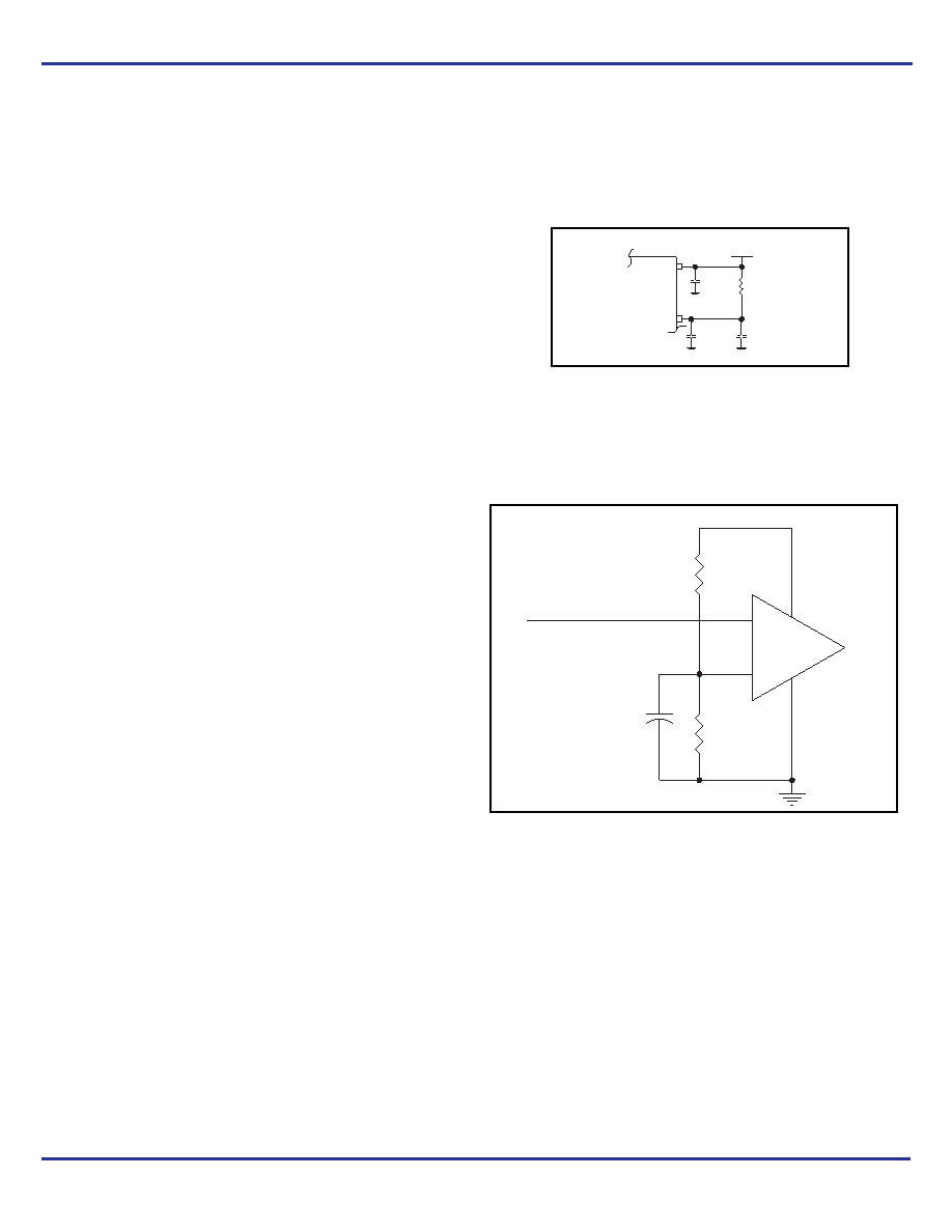
Wiring the Differential Input to Accept Single Ended Levels
Figure 2 shows how the differential input can be wired to accept
single ended levels. The reference voltage V_REF = VDD/2 is
generated by the bias resistors R1, R2 and C1. This bias circuit
should be located as close as possible to the input pin. The ratio of
R1 and R2 might need to be adjusted to position the V_REF in the
center of the input voltage swing. For example, if the input clock swing
is only 2.5V and VDD = 3.3V, V_REF should be 1.25V and R2/R1 =
0.609.
Figure 2. Single-Ended Signal Driving Differential Input
Recommendations for Unused Input and Output Pins
Inputs:
CLK/nCLK Inputs
For applications not requiring the use of the differential input, both
CLK and nCLK can be left floating. Though not required, but for
additional protection, a 1k
resistor can be tied from CLK to ground.
LVCMOS Control Pins
All control pins have internal pullups or pulldowns; additional
resistance is not required but can be added for additional protection.
A 1k
resistor can be used.
Outputs:
LVCMOS Outputs
All unused LVCMOS output can be left floating. There should be no
trace attached.
VDD
VDDA
3.3V or 2.5V
10
10F
.01F
V_REF
Single Ended Clock Input
VDD
CLKx
nCLKx
R1
1K
C1
0.1u
R2
1K
相关PDF资料 |
PDF描述 |
|---|---|
| V375A3V3H200B | CONVERTER MOD DC/DC 3.3V 200W |
| ICS8633AF-01LF | IC BUFFER ZD 2-3 LVPECL 28-SSOP |
| V375A3V3H200BG2 | CONVERTER MOD DC/DC 3.3V 200W |
| VI-2WJ-MY-F4 | CONVERTER MOD DC/DC 36V 50W |
| V375A3V3H200BG | CONVERTER MOD DC/DC 3.3V 200W |
相关代理商/技术参数 |
参数描述 |
|---|---|
| ICS87004AGLFT | 功能描述:IC CLOCK GEN ZD 1:4 24-TSSOP RoHS:是 类别:集成电路 (IC) >> 时钟/计时 - 时钟发生器,PLL,频率合成器 系列:HiPerClockS™ 标准包装:1,000 系列:- 类型:时钟/频率合成器,扇出分配 PLL:- 输入:- 输出:- 电路数:- 比率 - 输入:输出:- 差分 - 输入:输出:- 频率 - 最大:- 除法器/乘法器:- 电源电压:- 工作温度:- 安装类型:表面贴装 封装/外壳:56-VFQFN 裸露焊盘 供应商设备封装:56-VFQFP-EP(8x8) 包装:带卷 (TR) 其它名称:844S012AKI-01LFT |
| ICS87004BG-03LF | 功能描述:IC CLOCK DIVIDER MUX 2:4 20TSSOP RoHS:是 类别:集成电路 (IC) >> 时钟/计时 - 时钟缓冲器,驱动器 系列:HiPerClockS™ 标准包装:74 系列:- 类型:扇出缓冲器(分配) 电路数:1 比率 - 输入:输出:1:10 差分 - 输入:输出:是/是 输入:HCSL, LVCMOS, LVDS, LVPECL, LVTTL 输出:HCSL,LVDS 频率 - 最大:400MHz 电源电压:3 V ~ 3.6 V 工作温度:-40°C ~ 85°C 安装类型:表面贴装 封装/外壳:32-VFQFN 裸露焊盘 供应商设备封装:32-QFN(5x5) 包装:管件 |
| ICS87004BG-03LFT | 功能描述:IC CLOCK DIVIDER MUX 2:4 20TSSOP RoHS:是 类别:集成电路 (IC) >> 时钟/计时 - 时钟缓冲器,驱动器 系列:HiPerClockS™ 标准包装:74 系列:- 类型:扇出缓冲器(分配) 电路数:1 比率 - 输入:输出:1:10 差分 - 输入:输出:是/是 输入:HCSL, LVCMOS, LVDS, LVPECL, LVTTL 输出:HCSL,LVDS 频率 - 最大:400MHz 电源电压:3 V ~ 3.6 V 工作温度:-40°C ~ 85°C 安装类型:表面贴装 封装/外壳:32-VFQFN 裸露焊盘 供应商设备封装:32-QFN(5x5) 包装:管件 |
| ICS87004BGI-03LF | 功能描述:IC CLOCK DIVIDER MUX 2:4 20TSSOP RoHS:是 类别:集成电路 (IC) >> 时钟/计时 - 时钟缓冲器,驱动器 系列:HiPerClockS™ 标准包装:74 系列:- 类型:扇出缓冲器(分配) 电路数:1 比率 - 输入:输出:1:10 差分 - 输入:输出:是/是 输入:HCSL, LVCMOS, LVDS, LVPECL, LVTTL 输出:HCSL,LVDS 频率 - 最大:400MHz 电源电压:3 V ~ 3.6 V 工作温度:-40°C ~ 85°C 安装类型:表面贴装 封装/外壳:32-VFQFN 裸露焊盘 供应商设备封装:32-QFN(5x5) 包装:管件 |
| ICS87004BGI-03LFT | 功能描述:IC CLOCK DIVIDER MUX 2:4 20TSSOP RoHS:是 类别:集成电路 (IC) >> 时钟/计时 - 时钟缓冲器,驱动器 系列:HiPerClockS™ 标准包装:74 系列:- 类型:扇出缓冲器(分配) 电路数:1 比率 - 输入:输出:1:10 差分 - 输入:输出:是/是 输入:HCSL, LVCMOS, LVDS, LVPECL, LVTTL 输出:HCSL,LVDS 频率 - 最大:400MHz 电源电压:3 V ~ 3.6 V 工作温度:-40°C ~ 85°C 安装类型:表面贴装 封装/外壳:32-VFQFN 裸露焊盘 供应商设备封装:32-QFN(5x5) 包装:管件 |
发布紧急采购,3分钟左右您将得到回复。