- 您现在的位置:买卖IC网 > PDF目录8988 > ICS87004AGLFT (IDT, Integrated Device Technology Inc)IC CLOCK GEN ZD 1:4 24-TSSOP PDF资料下载
参数资料
| 型号: | ICS87004AGLFT |
| 厂商: | IDT, Integrated Device Technology Inc |
| 文件页数: | 13/15页 |
| 文件大小: | 0K |
| 描述: | IC CLOCK GEN ZD 1:4 24-TSSOP |
| 标准包装: | 2,500 |
| 系列: | HiPerClockS™ |
| 类型: | 时钟发生器,扇出配送,多路复用器,零延迟缓冲器 |
| PLL: | 带旁路 |
| 输入: | HCSL,LVDS,LVHSTL,LVPECL,SSTL |
| 输出: | LVCMOS,LVTTL |
| 电路数: | 1 |
| 比率 - 输入:输出: | 2:4 |
| 差分 - 输入:输出: | 是/无 |
| 频率 - 最大: | 250MHz |
| 除法器/乘法器: | 是/是 |
| 电源电压: | 2.375 V ~ 3.465 V |
| 工作温度: | 0°C ~ 70°C |
| 安装类型: | 表面贴装 |
| 封装/外壳: | 24-TSSOP(0.173",4.40mm 宽) |
| 供应商设备封装: | 24-TSSOP |
| 包装: | 带卷 (TR) |
| 其它名称: | 87004AGLFT |
ICS87004AG REVISION C DECEMBER 1, 2009
7
2009 Integrated Device Technology, Inc.
ICS87004 Data Sheet
1:4, DIFFERENTIAL-TO-LVCMOS/LVTTL ZERO DELAY CLOCK GENERATOR
AC Electrical Characteristics
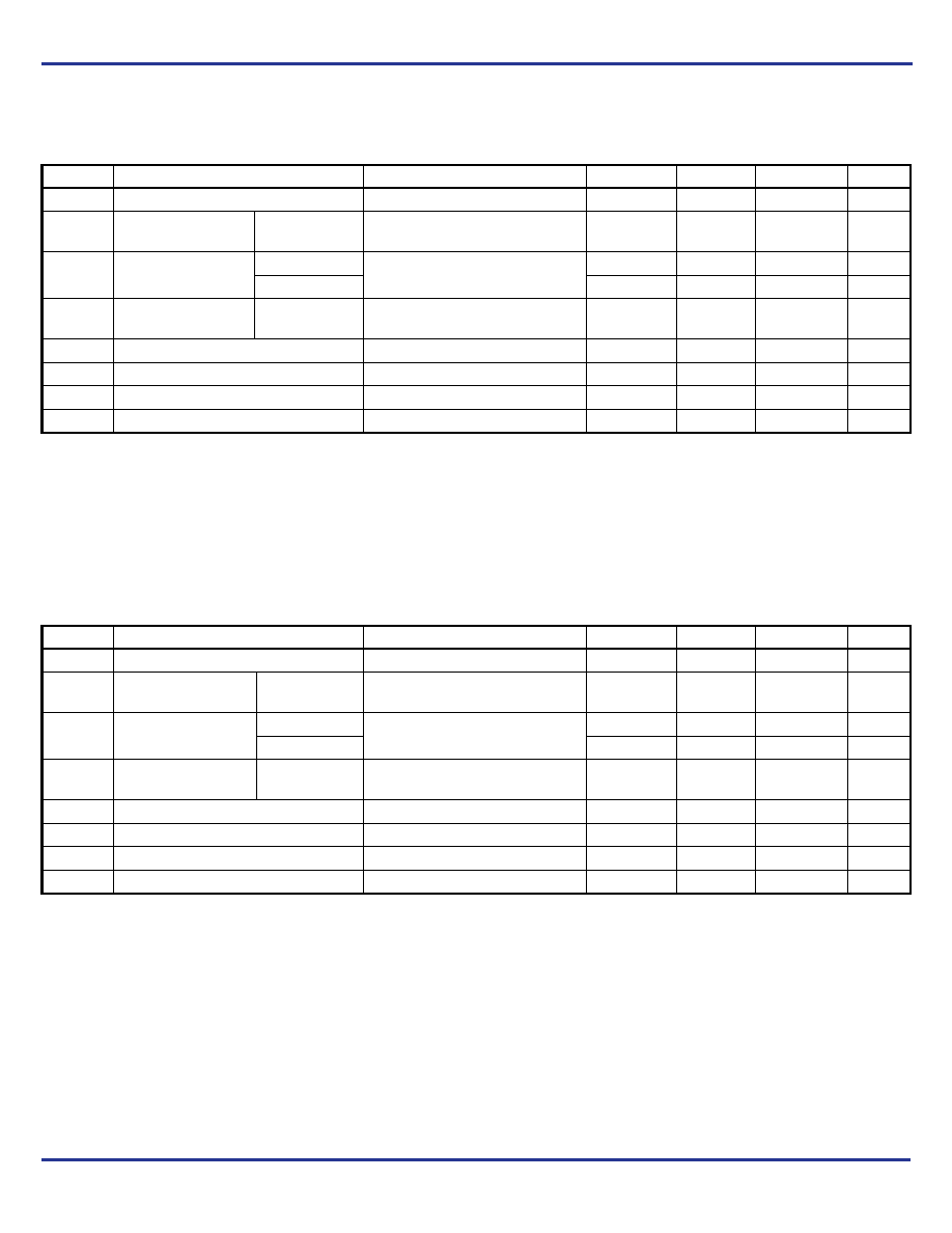
Table 5A. AC Characteristics, VDD = VDDO = 3.3V ± 5%, TA = 0°C to 70°C
NOTE: Electrical parameters are guaranteed over the specified ambient operating temperature range, which is established when the device is
mounted in a test socket with maintained transverse airflow greater than 500 lfpm. The device will meet specifications after thermal equilibrium
has been reached under these conditions.
NOTE 1: Measured from the differential input crossing point to the output at VDDO/2.
NOTE 2: Defined as the time difference between the input reference clock and the average feedback input signal when the PLL is locked and
the input reference frequency is stable.
NOTE 3: Defined as skew between outputs at the same supply voltage and with equal load conditions. Measured at VDDO/2.
NOTE 4: This parameter is defined in accordance with JEDEC Standard 65.
Table 5B. AC Characteristics, VDD = VDDO = 2.5V ± 5%, TA = 0°C to 70°C
NOTE: Electrical parameters are guaranteed over the specified ambient operating temperature range, which is established when the device is
mounted in a test socket with maintained transverse airflow greater than 500 lfpm. The device will meet specifications after thermal equilibrium
has been reached under these conditions.
NOTE 1: Measured from the differential input crossing point to the output at VDDO/2.
NOTE 2: Defined as the time difference between the input reference clock and the average feedback input signal, when the PLL is locked and
the input reference frequency is stable.
NOTE 3: Defined as skew between outputs at the same supply voltage and with equal load conditions. Measured at VDDO/2.
NOTE 4: This parameter is defined in accordance with JEDEC Standard 65.
Symbol
Parameter
Test Conditions
Minimum
Typical
Maximum
Units
fMAX
Output Frequency
15.625
250
MHz
tPD
Propagation Delay;
NOTE 1
CLK0, nCLK0
CLK1, nCLK1
PLL_SEL = 0V, f
≤ 250MHz,
Qx ÷ 2
56.2
ns
t()
Static Phase Offset;
NOTE 2, 4
CLK0, nCLK0
PLL_SEL = 3.3V,
fREF ≤ 167MHz, Qx ÷ 1
-75
50
175
ps
CLK1, nCLK1
-190
-65
175
ps
tsk(o)
Output Skew;
NOTE 3, 4
CLK0, nCLK0
CLK1, nCLK1
PLL_SEL = 0V
40
50
ps
tjit(cc)
Cycle-to-Cycle Jitter; NOTE 4
fOUT > 40MHz
30
45
ps
tL
PLL Lock Time
1ms
tR / tF
Output Rise/Fall Time
20% to 80%
400
800
ps
odc
Output Duty Cycle
40
50
60
%
Symbol
Parameter
Test Conditions
Minimum
Typical
Maximum
Units
fMAX
Output Frequency
15.625
250
MHz
tPD
Propagation Delay;
NOTE 1
CLK0, nCLK0
CLK1, nCLK1
PLL_SEL = 0V, f
≤ 250MHz,
Qx ÷ 2
5.3
6.9
ns
t()
Static Phase Offset;
NOTE 2, 4
CLK0, nCLK0
PLL_SEL = 2.5V,
fREF ≤ 167MHz, Qx ÷ 1
-175
-25
125
ps
CLK1, nCLK1
-290
-115
125
ps
tsk(o)
Output Skew;
NOTE 3, 4
CLK0, nCLK0
CLK1, nCLK1
PLL_SEL = 0V
40
45
ps
tjit(cc)
Cycle-to-Cycle Jitter; NOTE 4
fOUT > 40MHz
35
45
ps
tL
PLL Lock Time
1ms
tR / tF
Output Rise/Fall Time
20% to 80%
400
700
ps
odc
Output Duty Cycle
44
50
56
%
相关PDF资料 |
PDF描述 |
|---|---|
| VI-J4J-MZ-F2 | CONVERTER MOD DC/DC 36V 25W |
| VI-BNP-MV-F4 | CONVERTER MOD DC/DC 13.8V 150W |
| VI-BNP-MV-F3 | CONVERTER MOD DC/DC 13.8V 150W |
| AD5318ARUZ | IC DAC 10BIT OCTAL W/BUF 16TSSOP |
| VI-BNP-MV-F2 | CONVERTER MOD DC/DC 13.8V 150W |
相关代理商/技术参数 |
参数描述 |
|---|---|
| ICS87004BG-03LF | 功能描述:IC CLOCK DIVIDER MUX 2:4 20TSSOP RoHS:是 类别:集成电路 (IC) >> 时钟/计时 - 时钟缓冲器,驱动器 系列:HiPerClockS™ 标准包装:74 系列:- 类型:扇出缓冲器(分配) 电路数:1 比率 - 输入:输出:1:10 差分 - 输入:输出:是/是 输入:HCSL, LVCMOS, LVDS, LVPECL, LVTTL 输出:HCSL,LVDS 频率 - 最大:400MHz 电源电压:3 V ~ 3.6 V 工作温度:-40°C ~ 85°C 安装类型:表面贴装 封装/外壳:32-VFQFN 裸露焊盘 供应商设备封装:32-QFN(5x5) 包装:管件 |
| ICS87004BG-03LFT | 功能描述:IC CLOCK DIVIDER MUX 2:4 20TSSOP RoHS:是 类别:集成电路 (IC) >> 时钟/计时 - 时钟缓冲器,驱动器 系列:HiPerClockS™ 标准包装:74 系列:- 类型:扇出缓冲器(分配) 电路数:1 比率 - 输入:输出:1:10 差分 - 输入:输出:是/是 输入:HCSL, LVCMOS, LVDS, LVPECL, LVTTL 输出:HCSL,LVDS 频率 - 最大:400MHz 电源电压:3 V ~ 3.6 V 工作温度:-40°C ~ 85°C 安装类型:表面贴装 封装/外壳:32-VFQFN 裸露焊盘 供应商设备封装:32-QFN(5x5) 包装:管件 |
| ICS87004BGI-03LF | 功能描述:IC CLOCK DIVIDER MUX 2:4 20TSSOP RoHS:是 类别:集成电路 (IC) >> 时钟/计时 - 时钟缓冲器,驱动器 系列:HiPerClockS™ 标准包装:74 系列:- 类型:扇出缓冲器(分配) 电路数:1 比率 - 输入:输出:1:10 差分 - 输入:输出:是/是 输入:HCSL, LVCMOS, LVDS, LVPECL, LVTTL 输出:HCSL,LVDS 频率 - 最大:400MHz 电源电压:3 V ~ 3.6 V 工作温度:-40°C ~ 85°C 安装类型:表面贴装 封装/外壳:32-VFQFN 裸露焊盘 供应商设备封装:32-QFN(5x5) 包装:管件 |
| ICS87004BGI-03LFT | 功能描述:IC CLOCK DIVIDER MUX 2:4 20TSSOP RoHS:是 类别:集成电路 (IC) >> 时钟/计时 - 时钟缓冲器,驱动器 系列:HiPerClockS™ 标准包装:74 系列:- 类型:扇出缓冲器(分配) 电路数:1 比率 - 输入:输出:1:10 差分 - 输入:输出:是/是 输入:HCSL, LVCMOS, LVDS, LVPECL, LVTTL 输出:HCSL,LVDS 频率 - 最大:400MHz 电源电压:3 V ~ 3.6 V 工作温度:-40°C ~ 85°C 安装类型:表面贴装 封装/外壳:32-VFQFN 裸露焊盘 供应商设备封装:32-QFN(5x5) 包装:管件 |
| ICS87008AGI | 制造商:INT_CIR_SYS 功能描述: |
发布紧急采购,3分钟左右您将得到回复。