- 您现在的位置:买卖IC网 > PDF目录377124 > ICS8741004 (Integrated Device Technology, Inc.) DIFFERENTIAL-TO-LVDS/0.7V DIFFERENTIAL PCI EXPRESS⑩ JITTER ATTENUATOR PDF资料下载
参数资料
| 型号: | ICS8741004 |
| 厂商: | Integrated Device Technology, Inc. |
| 英文描述: | DIFFERENTIAL-TO-LVDS/0.7V DIFFERENTIAL PCI EXPRESS⑩ JITTER ATTENUATOR |
| 中文描述: | DIFFERENTIAL-TO-LVDS/0.7V微分的PCI Express⑩抖动衰减器 |
| 文件页数: | 9/17页 |
| 文件大小: | 715K |
| 代理商: | ICS8741004 |
ICS8741004
DIFFERENTIAL-TO-LVDS/0.7V DIFFERENTIAL PCI EXPRESS JITTER ATTENUATOR
IDT / ICS
PCI EXPRESS JITTER ATTENUATOR
9
ICS8741004AG REV. AAUGUST 3, 2007
Application Information
Power Supply Filtering Technique
As in any high speed analog circuitry, the power supply pins are
vulnerable to random noise. The ICS8741004 provides separate
power supplies to isolate any high switching noise from the outputs
to the internal PLL. V
DD,
V
DDA
and V
DDO
should be individually
connected to the power supply plane through vias, and bypass
capacitors should be used for each pin. To achieve optimum jitter
performance, power supply isolation is required.
Figure 1
illustrates how a 10
resistor along with a 10
μ
F and a 0.01
μ
F
bypass capacitor should be connected to each V
DDA
pin.
Figure 1. Power Supply Filtering
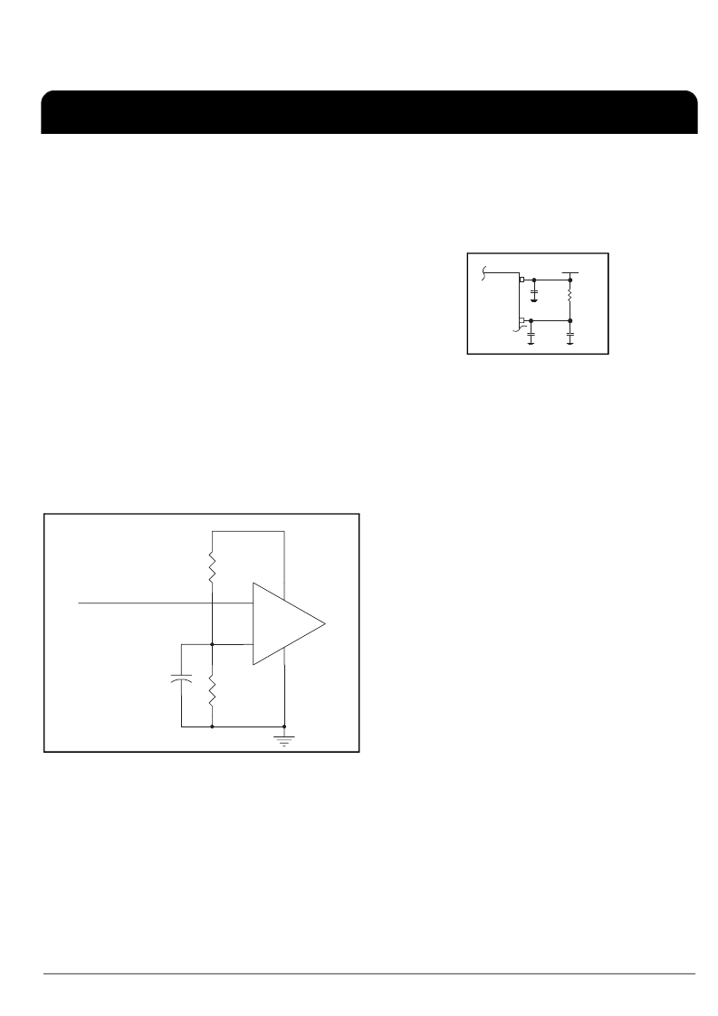
Wiring the Differential Input to Accept Single Ended Levels
Figure 2
shows how the differential input can be wired to accept
single ended levels. The reference voltage V_REF = V
DD
/2 is
generated by the bias resistors R1, R2 and C1. This bias circuit
should be located as close as possible to the input pin. The ratio of
R1 and R2 might need to be adjusted to position the V_REF in the
center of the input voltage swing. For example, if the input clock
swing is only 2.5V and V
DD
= 3.3V, V_REF should be 1.25V and
R2/R1 = 0.609.
Figure 2. Single-Ended Signal Driving Differential Input
V
DD
V
DDA
3.3V
10
10μF
.01μF
.01μF
V_REF
Single Ended Clock Input
V
DD
CLK
nCLK
R1
1K
C1
0.1u
R2
1K
相关PDF资料 |
PDF描述 |
|---|---|
| ICS8741004AG | DIFFERENTIAL-TO-LVDS/0.7V DIFFERENTIAL PCI EXPRESS⑩ JITTER ATTENUATOR |
| ICS8741004AGLF | DIFFERENTIAL-TO-LVDS/0.7V DIFFERENTIAL PCI EXPRESS⑩ JITTER ATTENUATOR |
| ICS98ULPA877A | 1.8V Low-Power Wide-Range Frequency Clock Driver |
| ICS98ULPA877AKLF-T | 1.8V Low-Power Wide-Range Frequency Clock Driver |
| ICS9DB102YFLFT | 2 Output PCI Express Buffer with CLKREQ Function |
相关代理商/技术参数 |
参数描述 |
|---|---|
| ICS8741004AGLF | 功能描述:IC PCI EXPRSS/JITT ATTEN 24TSSOP RoHS:是 类别:集成电路 (IC) >> 时钟/计时 - 专用 系列:HiPerClockS™, FemtoClock™, PCI Express® (PCIe) 标准包装:1 系列:- 类型:时钟/频率发生器,多路复用器 PLL:是 主要目的:存储器,RDRAM 输入:晶体 输出:LVCMOS 电路数:1 比率 - 输入:输出:1:2 差分 - 输入:输出:无/是 频率 - 最大:400MHz 电源电压:3 V ~ 3.6 V 工作温度:0°C ~ 85°C 安装类型:表面贴装 封装/外壳:16-TSSOP(0.173",4.40mm 宽) 供应商设备封装:16-TSSOP 包装:Digi-Reel® 其它名称:296-6719-6 |
| ICS8741004AGLFT | 功能描述:IC PCI EXPRSS/JITT ATTEN 24TSSOP RoHS:是 类别:集成电路 (IC) >> 时钟/计时 - 专用 系列:HiPerClockS™, FemtoClock™, PCI Express® (PCIe) 标准包装:1,500 系列:- 类型:时钟缓冲器/驱动器 PLL:是 主要目的:- 输入:- 输出:- 电路数:- 比率 - 输入:输出:- 差分 - 输入:输出:- 频率 - 最大:- 电源电压:3.3V 工作温度:0°C ~ 70°C 安装类型:表面贴装 封装/外壳:28-SSOP(0.209",5.30mm 宽) 供应商设备封装:28-SSOP 包装:带卷 (TR) 其它名称:93786AFT |
| ICS8741004BGILF | 功能描述:IC PCI EXPRSS/JITT ATTEN 24TSSOP RoHS:是 类别:集成电路 (IC) >> 时钟/计时 - 专用 系列:HiPerClockS™, FemtoClock™, PCI Express® (PCIe) 标准包装:1,500 系列:- 类型:时钟缓冲器/驱动器 PLL:是 主要目的:- 输入:- 输出:- 电路数:- 比率 - 输入:输出:- 差分 - 输入:输出:- 频率 - 最大:- 电源电压:3.3V 工作温度:0°C ~ 70°C 安装类型:表面贴装 封装/外壳:28-SSOP(0.209",5.30mm 宽) 供应商设备封装:28-SSOP 包装:带卷 (TR) 其它名称:93786AFT |
| ICS8741004BGILFT | 功能描述:IC PCI EXPRSS/JITT ATTEN 24TSSOP RoHS:是 类别:集成电路 (IC) >> 时钟/计时 - 专用 系列:HiPerClockS™, FemtoClock™, PCI Express® (PCIe) 标准包装:1,500 系列:- 类型:时钟缓冲器/驱动器 PLL:是 主要目的:- 输入:- 输出:- 电路数:- 比率 - 输入:输出:- 差分 - 输入:输出:- 频率 - 最大:- 电源电压:3.3V 工作温度:0°C ~ 70°C 安装类型:表面贴装 封装/外壳:28-SSOP(0.209",5.30mm 宽) 供应商设备封装:28-SSOP 包装:带卷 (TR) 其它名称:93786AFT |
| ICS874208BKILF | 制造商:Integrated Device Technology Inc 功能描述:IC CLK BUFFER/DIVIDER 32VFQFN |
发布紧急采购,3分钟左右您将得到回复。