- 您现在的位置:买卖IC网 > PDF目录8991 > ICS87972DYI-147LFT (IDT, Integrated Device Technology Inc)IC CLK MULT/ZD BUFFER 52-LQFP PDF资料下载
参数资料
| 型号: | ICS87972DYI-147LFT |
| 厂商: | IDT, Integrated Device Technology Inc |
| 文件页数: | 1/17页 |
| 文件大小: | 0K |
| 描述: | IC CLK MULT/ZD BUFFER 52-LQFP |
| 标准包装: | 500 |
| 系列: | HiPerClockS™ |
| 类型: | 时钟倍频器,零延迟缓冲器 |
| PLL: | 带旁路 |
| 输入: | LVCMOS,LVTTL,晶体 |
| 输出: | LVCMOS,LVTTL |
| 电路数: | 1 |
| 比率 - 输入:输出: | 3:12 |
| 差分 - 输入:输出: | 无/无 |
| 频率 - 最大: | 150MHz |
| 除法器/乘法器: | 是/无 |
| 电源电压: | 3.135 V ~ 3.465 V |
| 工作温度: | -40°C ~ 85°C |
| 安装类型: | 表面贴装 |
| 封装/外壳: | 52-LQFP |
| 供应商设备封装: | 52-TQFP(10x10) |
| 包装: | 带卷 (TR) |
| 其它名称: | 87972DYI-147LFT |
LOW SKEW, 1-TO-12 LVCMOS/LVTTL CLOCK MULTIPLIER/
ZERO DELAY BUFFER
ICS87972I-147
IDT / ICS LVCMOS CLOCK MULTIPLIER/ZERO DELAY BUFFER
1
ICS87972DYI-147 REV. A JUNE 5, 2008
General Description
The ICS87972I-147 is a low skew, LVCMOS/LVTTL
Clock Generator and a member of the HiPerClockS
family of High Performance Clock Solutions from
ICS. The ICS87972I-147 has three selectable inputs
and provides 14 LVCMOS/LVTTL outputs.
The ICS87972I-147 is a highly flexible device. Using the crystal
oscillator input, it can be used to generate clocks for a system. All
of these clocks can be the same frequency or the device can be
configured to generate up to three different frequencies among the
three output banks. Using one of the single ended inputs, the
ICS87972I-147 can be used as a zero delay buffer/multiplier/
divider in clock distribution applications.
The three output banks and feedback output each have their own
output dividers which allows the device to generate a multitude of
different bank frequency ratios and output-to-input frequency
ratios. In addition, 2 outputs in Bank C (QC2, QC3) can be select-
ed to be inverting or non-inverting. The output frequency range is
10MHz to 150MHz. Input frequency range is 6MHz to 150MHz.
The ICS87972I-147 also has a QSYNC output which can be used
or system synchronization purposes. It monitors Bank A and Bank
C outputs and goes low one period of the faster clock prior to
coincident rising edges of Bank A and Bank C clocks. QSYNC
then goes high again when the coincident rising edges of Bank A
and Bank C occur. This feature is used primarily in applications
where Bank A and Bank C are running at different frequencies,
and is particularly useful when they are running at non-integer
multiples of one another.
Example Applications:
1.System Clock generator: Use a 16.66 MHz Crystal to generate
eight 33.33MHz copies for PCI and four 100MHz copies for the
CPU or PCI-X.
2.Line Card Multiplier: Multiply 19.44MHz from a back plane to
77.76MHz for the line Card ASICs and Serdes.
3.Zero Delay buffer for Synchronous memory: Fan out up to
twelve 100MHz copies from a memory controller reference
clock to the memory chips on a memory module with zero delay.
Features
Fully integrated PLL
Fourteen LVCMOS/LVTTL outputs; (12)clocks, (1)feedback,
(1)sync
Selectable crystal oscillator interface or LVCMOS/LVTTL
reference clock inputs
CLK0, CLK1 can accept the following input levels:
LVCMOS or LVTTL
Output frequency range: 10MHz to 150MHz
VCO range: 240MHz to 500MHz
Output skew: 200ps (maximum)
Cycle-to-cycle jitter, (all banks ÷4): 55ps (maximum)
Full 3.3V supply voltage
-40°C to 85°C ambient operating temperature
Compatible with PowerPCand PentiumMicroprocessors
Available in both standard (RoHS 5) and lead-free (RoHS 6)
packages.
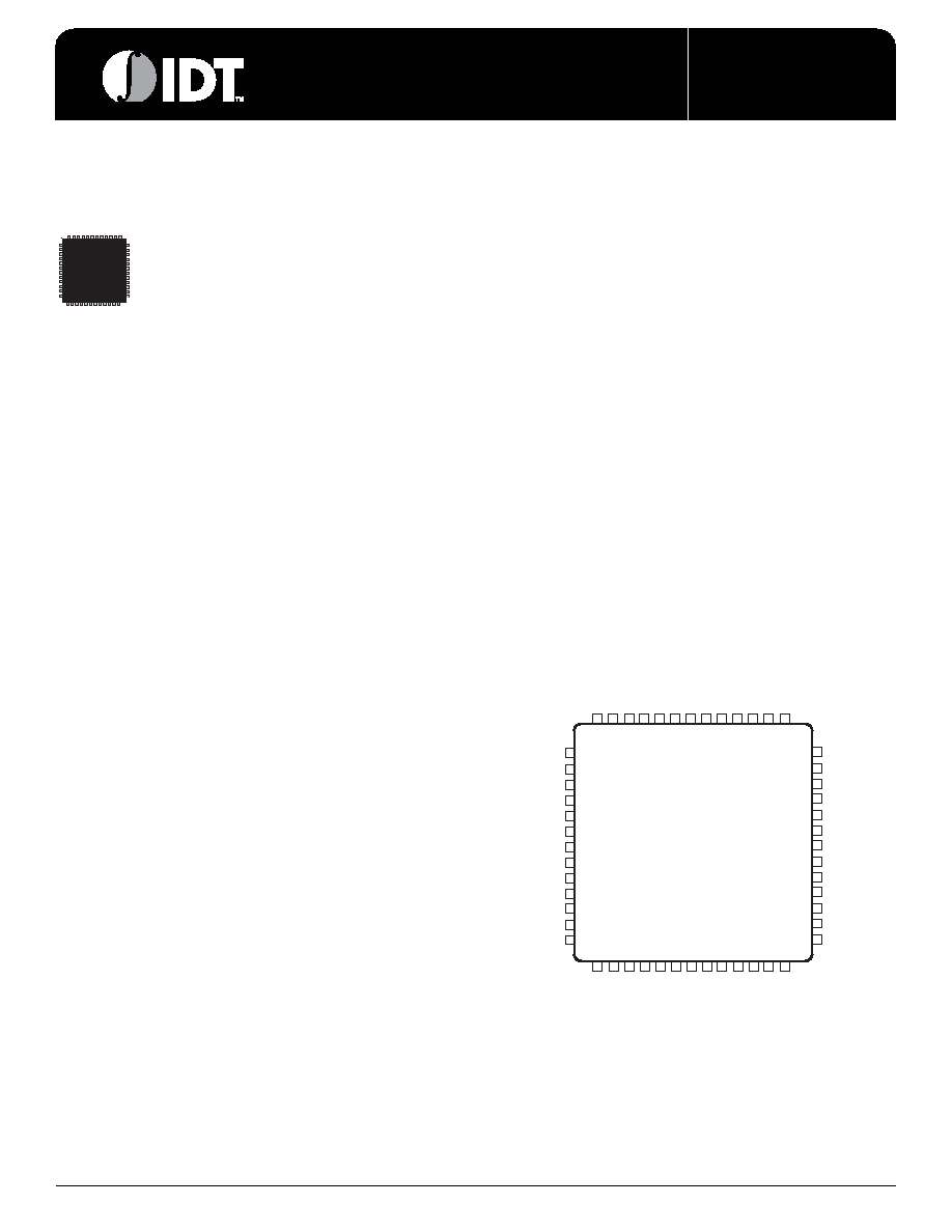
HiPerClockS
ICS
1
2 3
4 5 6
7 8 9 10 11 12 13
40
41
42
43
44
45
46
47
48
49
50
51
52
21
22
23
24
25
26
20
19
18
17
16
15
14
32
33
34
35
36
37
38
39
31 30 29 28 27
FSEL_B1
FSEL_B0
FSEL_A1
FSEL_A0
QA3
VDDO
QA2
GNDO
QA1
VDDO
QA0
GNDO
VCO_SEL
FSEL_FB1
QSYNC
GNDO
QC0
VDDO
INV_CLK
QC1
FSEL_C0
FSEL_C1
QC2
VDDO
QC3
GNDO
GNDI
V
DDA
nMR/OE
FRZ_CLK
FRZ_DATA
FSEL_FB2
PLL_SEL
REF_SEL
CLK_SEL
CLK0
CLK1
XTAL1
XTAL2
GNDO
QB0
V
DDO
QB1
GNDO
QB2
V
DDO
QB3
FSEL_FB0
EXT_FB
GNDO
QFB
V
DD
Pin Assignment
ICS87972I-147
52-Lead LQFP
10mm x 10mm x 1.4mm package body
Y Package
Top View
相关PDF资料 |
PDF描述 |
|---|---|
| AD5664BCPZ-REEL7 | IC DAC NANO 16BIT QUAD 10-LFCSP |
| D38999/26MC4SE | CONN PLUG 4POS STRAIGHT W/SCKT |
| AD7304BRZ | IC DAC 8BIT QUAD R-R 16-SOIC |
| LTC1452CS8#PBF | IC D/A CONV 12BIT R-R 8-SOIC |
| SY100EPT20VKG | IC TRANSLATOR 3.3/5V 8-MSOP |
相关代理商/技术参数 |
参数描述 |
|---|---|
| ICS87972DYILF | 功能描述:IC CLK MULT/ZD BUFFER 52-LQFP RoHS:是 类别:集成电路 (IC) >> 时钟/计时 - 时钟发生器,PLL,频率合成器 系列:HiPerClockS™ 标准包装:1,000 系列:- 类型:时钟/频率合成器,扇出分配 PLL:- 输入:- 输出:- 电路数:- 比率 - 输入:输出:- 差分 - 输入:输出:- 频率 - 最大:- 除法器/乘法器:- 电源电压:- 工作温度:- 安装类型:表面贴装 封装/外壳:56-VFQFN 裸露焊盘 供应商设备封装:56-VFQFP-EP(8x8) 包装:带卷 (TR) 其它名称:844S012AKI-01LFT |
| ICS87972DYILFT | 功能描述:IC CLK MULT/ZD BUFFER 52-LQFP RoHS:是 类别:集成电路 (IC) >> 时钟/计时 - 时钟发生器,PLL,频率合成器 系列:HiPerClockS™ 标准包装:1,000 系列:- 类型:时钟/频率合成器,扇出分配 PLL:- 输入:- 输出:- 电路数:- 比率 - 输入:输出:- 差分 - 输入:输出:- 频率 - 最大:- 除法器/乘法器:- 电源电压:- 工作温度:- 安装类型:表面贴装 封装/外壳:56-VFQFN 裸露焊盘 供应商设备封装:56-VFQFP-EP(8x8) 包装:带卷 (TR) 其它名称:844S012AKI-01LFT |
| ICS87973DYI-147LF | 功能描述:IC CLK MULT/ZD BUFFER 52TQFP RoHS:是 类别:集成电路 (IC) >> 时钟/计时 - 时钟发生器,PLL,频率合成器 系列:HiPerClockS™ 标准包装:1,000 系列:- 类型:时钟/频率合成器,扇出分配 PLL:- 输入:- 输出:- 电路数:- 比率 - 输入:输出:- 差分 - 输入:输出:- 频率 - 最大:- 除法器/乘法器:- 电源电压:- 工作温度:- 安装类型:表面贴装 封装/外壳:56-VFQFN 裸露焊盘 供应商设备封装:56-VFQFP-EP(8x8) 包装:带卷 (TR) 其它名称:844S012AKI-01LFT |
| ICS87973DYI-147LFT | 功能描述:IC CLK MULT/ZD BUFFER 52TQFP RoHS:是 类别:集成电路 (IC) >> 时钟/计时 - 时钟发生器,PLL,频率合成器 系列:HiPerClockS™ 标准包装:1,000 系列:- 类型:时钟/频率合成器,扇出分配 PLL:- 输入:- 输出:- 电路数:- 比率 - 输入:输出:- 差分 - 输入:输出:- 频率 - 最大:- 除法器/乘法器:- 电源电压:- 工作温度:- 安装类型:表面贴装 封装/外壳:56-VFQFN 裸露焊盘 供应商设备封装:56-VFQFP-EP(8x8) 包装:带卷 (TR) 其它名称:844S012AKI-01LFT |
| ICS87973DYILF | 功能描述:IC CLK MULT/ZD BUFFER 52-LQFP RoHS:是 类别:集成电路 (IC) >> 时钟/计时 - 时钟发生器,PLL,频率合成器 系列:HiPerClockS™ 标准包装:2,000 系列:- 类型:PLL 频率合成器 PLL:是 输入:晶体 输出:时钟 电路数:1 比率 - 输入:输出:1:1 差分 - 输入:输出:无/无 频率 - 最大:1GHz 除法器/乘法器:是/无 电源电压:4.5 V ~ 5.5 V 工作温度:-20°C ~ 85°C 安装类型:表面贴装 封装/外壳:16-LSSOP(0.175",4.40mm 宽) 供应商设备封装:16-SSOP 包装:带卷 (TR) 其它名称:NJW1504V-TE1-NDNJW1504V-TE1TR |
发布紧急采购,3分钟左右您将得到回复。