- 您现在的位置:买卖IC网 > PDF目录67111 > ICS9112M-06 91 SERIES, PLL BASED CLOCK DRIVER, 5 TRUE OUTPUT(S), 0 INVERTED OUTPUT(S), PDSO8 PDF资料下载
参数资料
| 型号: | ICS9112M-06 |
| 元件分类: | 时钟及定时 |
| 英文描述: | 91 SERIES, PLL BASED CLOCK DRIVER, 5 TRUE OUTPUT(S), 0 INVERTED OUTPUT(S), PDSO8 |
| 封装: | 0.150 INCH, SOIC-8 |
| 文件页数: | 1/8页 |
| 文件大小: | 209K |
| 代理商: | ICS9112M-06 |
Integrated
Circuit
Systems, Inc.
General Description
Features
ICS9112-06/07
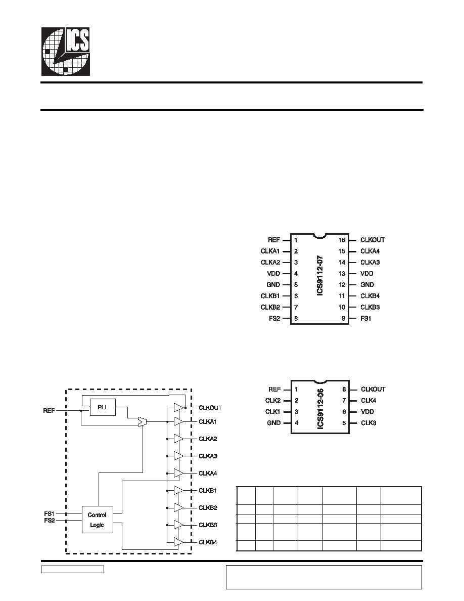
Block Diagram
Low Skew Output Buffer
9112-06/07 Rev H 1/22/99
Pin Configuration
16 pin SOIC
Zero input - output delay
Frequency range 25 - 75 MHz (3.3V), 30-90MHz (5.0V)
Less than 200 ps Jitter between outputs
Skew controlled outputs
Skew less than 250 ps between outputs
Available in 8 or 16 pin versions, 150 mil SOIC packages
3.3V ±10%, 5.0V±10% operation
The ICS9112 is a high performance, low skew, low jitter clock
driver. It uses a phase lock loop (PLL) technology to align, in
both phase and frequency, the REF input with the CLKOUT
signal. It is designed to distribute high speed clocks in PC
systems operating at speeds from 25 to
75 MHz (30 to 90mHz for 5V operation).
ICS9112 is a zero delay buffer that provides synchronization
between the input and output. The synchronization is
established via CLKOUT feed back to the input of the PLL.
Since the skew between the input and output is less than +/-
350 pS, the part acts as a zero delay buffer.
The ICS9112 comes in with two different options; dash 06
and dash 07. The dash 07 is available in a 16 pin 150 mil SOIC
package. It has two banks of four outputs controlled by two
address lines. Depending on the selected address line, bank B
or both banks can be put in a tri-state mode. In this mode, the
PLL is still running and only the output buffers are put in a
high impedance mode. The test mode shuts off the PLL and
connects the input directly to the output buffers (see table
below for functionality).
The dash 06 is an eight pin 150 mil SOIC package. It has five
output clocks. In the absence of REF input, both ICS9112-06
and -07 will be in the power down mode. In this mode, the
PLL is turned off and the output buffers are pulled low. Power
down mode provides the lowest power consumption for a
standby condition.
8 pin SOIC
2
S
F1
S
F
A
K
L
C
)
4
,
1
(
B
K
L
C
)
4
,
1
(
T
U
O
K
L
C
t
u
p
t
u
O
e
c
r
u
o
S
L
P
n
w
o
d
t
u
h
S
00
e
t
a
t
s
i
r
Te
t
a
t
s
i
r
Tn
e
v
i
r
DL
L
PN
01
n
e
v
i
r
De
t
a
t
s
i
r
Tn
e
v
i
r
DL
L
PN
10
t
s
e
T
e
d
o
M
t
s
e
T
e
d
o
M
t
s
e
T
e
d
o
M
F
E
RY
11
n
e
v
i
r
Dn
e
v
i
r
Dn
e
v
i
r
DL
L
PN
Functionality (-07)
ICS reserves the right to make changes in the device data identified in this publication
without further notice. ICS advises its customers to obtain the latest version of all device
data to verify that any information being relied upon by the customer is current and accurate.
相关PDF资料 |
PDF描述 |
|---|---|
| ICS9112YM-28-T | LOW SKEW CLOCK DRIVER, 5 TRUE OUTPUT(S), 0 INVERTED OUTPUT(S), PDSO8 |
| ICS9120M-45LF | 50 MHz, OTHER CLOCK GENERATOR, PDSO8 |
| ICS9120M-45 | 50 MHz, OTHER CLOCK GENERATOR, PDSO8 |
| ICS91305YGI-T | 91305 SERIES, PLL BASED CLOCK DRIVER, 4 TRUE OUTPUT(S), 0 INVERTED OUTPUT(S), PDSO8 |
| ICS91305YMI-T | 91305 SERIES, PLL BASED CLOCK DRIVER, 4 TRUE OUTPUT(S), 0 INVERTED OUTPUT(S), PDSO8 |
相关代理商/技术参数 |
参数描述 |
|---|---|
| ICS9112M-07 | 制造商:ICS 制造商全称:ICS 功能描述:Low Skew Output Buffer |
| ICS9112M-22 | 功能描述:IC CLK BUFFER DVR 133MHZ 8-SOIC RoHS:否 类别:集成电路 (IC) >> 时钟/计时 - 时钟缓冲器,驱动器 系列:- 标准包装:74 系列:- 类型:扇出缓冲器(分配) 电路数:1 比率 - 输入:输出:1:10 差分 - 输入:输出:是/是 输入:HCSL, LVCMOS, LVDS, LVPECL, LVTTL 输出:HCSL,LVDS 频率 - 最大:400MHz 电源电压:3 V ~ 3.6 V 工作温度:-40°C ~ 85°C 安装类型:表面贴装 封装/外壳:32-VFQFN 裸露焊盘 供应商设备封装:32-QFN(5x5) 包装:管件 |
| ICS9112M-31 | 制造商:ICS 制造商全称:ICS 功能描述:Frequency Generator for Fibre Channel Systems |
| ICS9112M-32 | 制造商:ICS 制造商全称:ICS 功能描述:Frequency Generator for Fibre Channel Systems |
| ICS9112M-33 | 功能描述:IC CLOCK DRIVER LO JITTER 8-SOIC RoHS:否 类别:集成电路 (IC) >> 时钟/计时 - 专用 系列:- 标准包装:28 系列:- 类型:时钟/频率发生器 PLL:是 主要目的:Intel CPU 服务器 输入:时钟 输出:LVCMOS 电路数:1 比率 - 输入:输出:3:22 差分 - 输入:输出:无/是 频率 - 最大:400MHz 电源电压:3.135 V ~ 3.465 V 工作温度:0°C ~ 85°C 安装类型:表面贴装 封装/外壳:64-TFSOP (0.240",6.10mm 宽) 供应商设备封装:64-TSSOP 包装:管件 |
发布紧急采购,3分钟左右您将得到回复。