- 您现在的位置:买卖IC网 > PDF目录9046 > ICS91309AGLF (IDT, Integrated Device Technology Inc)IC BUFFER ZD LOW JITTER 16-TSSOP PDF资料下载
参数资料
| 型号: | ICS91309AGLF |
| 厂商: | IDT, Integrated Device Technology Inc |
| 文件页数: | 1/10页 |
| 文件大小: | 0K |
| 描述: | IC BUFFER ZD LOW JITTER 16-TSSOP |
| 标准包装: | 96 |
| 类型: | 零延迟缓冲器 |
| PLL: | 带旁路 |
| 输入: | 时钟 |
| 输出: | 时钟 |
| 电路数: | 1 |
| 比率 - 输入:输出: | 1:9 |
| 差分 - 输入:输出: | 无/无 |
| 频率 - 最大: | 133MHz |
| 除法器/乘法器: | 无/无 |
| 电源电压: | 2.97 V ~ 3.63 V |
| 工作温度: | 0°C ~ 70°C |
| 安装类型: | 表面贴装 |
| 封装/外壳: | 16-TSSOP(0.173",4.40mm 宽) |
| 供应商设备封装: | 16-TSSOP |
| 包装: | 管件 |
| 其它名称: | 91309AGLF |
Integrated
Circuit
Systems, Inc.
General Description
Features
ICS91309
0093H—12/09/08
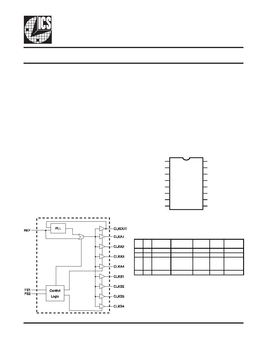
Block Diagram
High Performance Communication Buffer
Pin Configuration
Zero input - output delay
Frequency range 10 - 133 MHz (3.3V)
5V tolerant input REF
High loop filter bandwidth ideal for Spread Spectrum
applications.
Less than 125 ps cycle to cycle Jitter
Skew controlled outputs
Available in 16 pin, 150 mil SSOP, SOIC & 4.40mm
TSSOP packages
Skew: Group-to-Group: <215 ps
Skew within Group: <100 ps
Commercial temperature range: 0°C to +70°C
The ICS91309 is a high performance, low skew, low jitter
zero delay buffer.
It uses a phase lock loop (PLL)
technology to align, in both phase and frequency, the REF
input with the CLKOUT signal. It is designed to distribute
high speed clocks in communication systems operating
at speeds from 10 to 133 MHz.
The ICS91309 provides synchronization between the
input and output. The synchronization is established via
CLKOUT feed back to the input of the PLL. Since the skew
between the input and output is less than +/- 350 pS, the
part acts as a zero delay buffer.
ICS91309 has two banks of four outputs controlled by two
address lines. Depending on the selected address line,
bank B or both banks can be put in a tri-state mode. In this
mode, the PLL is still running and only the output buffers
are put in a high impedance mode. The test mode shuts
off the PLL and connects the input directly to the output
buffers (see table below for functionality).
ICS91309 comes in a 16-pin 150 mil SOIC, SSOP or
4.40mm TSSOP package. In the absence of REF input,
the device will enter a powerdown mode. In this mode, the
PLL is turned off and the output buffers are pulled low.
Power down mode provides the lowest power consumption
for a standby condition.
16 pin SSOP, SOIC & TSSOP
REF
CLKA1
CLKA2
VDD
GND
CLKB1
CLKB2
FS2
CLKOUT
CLKA4
CLKA3
VDD
GND
CLKB4
CLKB3
FS1
ICS91309
1
2
3
4
5
6
7
8
16
15
14
13
12
11
10
9
Functionality
FS2 FS1 CLKA(1:4) CLKB(1:4)
CLKOUT
Ouput
Source
PLL
Shutdown
0
Tristate
Driven
PLL
N
0
1
Driven
Tristate
Driven
PLL
N
10
PLL
Bypass
Mode
PLL Bypass
Mode
PLL
Bypass
Mode
REF
Y
1
Driven
PLL
N
相关PDF资料 |
PDF描述 |
|---|---|
| VE-JWM-MZ-F1 | CONVERTER MOD DC/DC 10V 25W |
| SL28SRC01BZIT | IC CLOCK PCIE GEN3/2 DIF 16TSSOP |
| VE-JWL-MZ-F4 | CONVERTER MOD DC/DC 28V 25W |
| ICS91718CMT | IC CLOCK GENERATOR LOW EMI 8SOIC |
| ICS91718CMLFT | IC CLOCK GENERATOR LOW EMI 8SOIC |
相关代理商/技术参数 |
参数描述 |
|---|---|
| ICS91309AGLFT | 功能描述:IC BUFFER ZD LOW JITTER 16-TSSOP RoHS:是 类别:集成电路 (IC) >> 时钟/计时 - 时钟发生器,PLL,频率合成器 系列:- 标准包装:2,000 系列:- 类型:PLL 时钟发生器 PLL:带旁路 输入:LVCMOS,LVPECL 输出:LVCMOS 电路数:1 比率 - 输入:输出:2:11 差分 - 输入:输出:是/无 频率 - 最大:240MHz 除法器/乘法器:是/无 电源电压:3.135 V ~ 3.465 V 工作温度:0°C ~ 70°C 安装类型:表面贴装 封装/外壳:32-LQFP 供应商设备封装:32-TQFP(7x7) 包装:带卷 (TR) |
| ICS91309FLF-T | 制造商:ICS 制造商全称:ICS 功能描述:High performance Communication Buffer |
| ICS91309GLF-T | 制造商:ICS 制造商全称:ICS 功能描述:High performance Communication Buffer |
| ICS91309MLF-T | 制造商:ICS 制造商全称:ICS 功能描述:High performance Communication Buffer |
| ICS9131 | 制造商:ICS 制造商全称:ICS 功能描述:32 KhZ Motherboard Frequency Generator |
发布紧急采购,3分钟左右您将得到回复。