- 您现在的位置:买卖IC网 > PDF目录67705 > ICS9148F-58 133.3 MHz, PROC SPECIFIC CLOCK GENERATOR, PDSO48 PDF资料下载
参数资料
| 型号: | ICS9148F-58 |
| 元件分类: | 时钟产生/分配 |
| 英文描述: | 133.3 MHz, PROC SPECIFIC CLOCK GENERATOR, PDSO48 |
| 封装: | 0.300 INCH, SSOP-48 |
| 文件页数: | 10/14页 |
| 文件大小: | 449K |
| 代理商: | ICS9148F-58 |
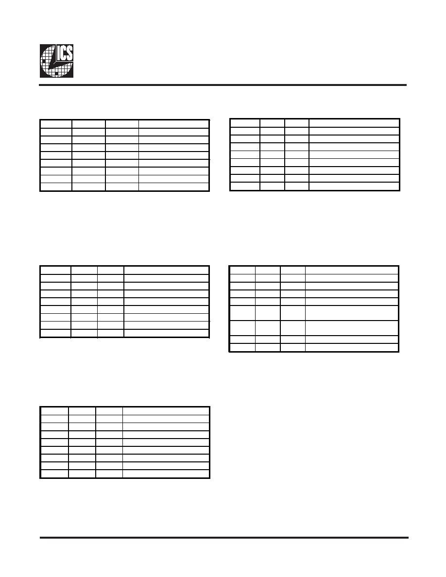
5
ICS9148-58
Byte 1: CPU,Active/Inactive Register
(1 = enable, 0 = disable)
Byte 2: PCIActive/Inactive Register
(1 = enable, 0 = disable)
Byte 3: SDRAMActive/Inactive Register
(1 = enable, 0 = disable)
Notes:
1. Inactive means outputs are held LOW and are disabled
from switching.
Notes:
1. Inactive means outputs are held LOW and are disabled
from switching.
Notes:
1. Inactive means outputs are held LOW and are disabled
from switching.
Bit
Pin #
PWD
Description
Bit 7
-
1
(Reserved)
Bit 6
-
1
(Reserved)
Bit 5
-
1
(Reserved)
Bit 4
-
1
(Reserved)
Bit 3
40
1
CPUCLK3 (Act/Inact)
Bit 2
41
1
CPUCLK2 (Act/Inact)
Bit 1
43
1
CPUCLK1 (Act/Inact)
Bit 0
44
1
CPUCLK0 (Act/Inact)
Bit
Pin #
PWD
Description
Bit 7
-
1
(Reserved)
Bit 6
7
1
PCICLK_F (Act/Inact)
Bit 5
15
1
AGP0 (Act/Inact)
Bit 4
14
1
PCICLK4 (Act/Inact)
Bit 3
12
1
PCICLK3 (Act/Inact)
Bit 2
11
1
PCICLK2 (Act/Inact)
Bit 1
10
1
PCICLK1 (Act/Inact)
Bit 0
8
1
PCICLK0(Act/Inact)
Bit
Pin #
PWD
Description
Bit 7
28
1
SDRAM7 (Act/Inact)
Bit 6
29
1
SDRAM6 (Act/Inact)
Bit 5
31
1
SDRAM5 (Act/Inact)
Bit 4
32
1
SDRAM4 (Act/Inact)
Bit 3
34
1
SDRAM3 (Act/Inact)
Bit 2
35
1
SDRAM2 (Act/Inact)
Bit 1
37
1
SDRAM1 (Act/Inact)
Bit 0
38
1
SDRAM0 (Act/Inact)
Byte 4: SDRAM Active/Inactive Register
(1 = enable, 0 = disable)
Byte5:Peripheral Active/InactiveRegister
(1 = enable, 0 = disable)
Notes:
1. Inactive means outputs are held LOW and are disabled
from switching.
Notes:
1. Inactive means outputs are held LOW and are disabled
from switching.
Bit
Pin #
PWD
Description
Bit 7
-
1
(Reserved)
Bit 6
-
1
(Reserved)
Bit 5
-
1
(Reserved)
Bit 4
-
1
(Reserved)
Bit 3
17
1
SDRAM11 (Act/Inact)
(Desktop Mode Only)
Bit 2
18
1
SDRAM10 (Act/Inact)
(Desktop Mode Only)
Bit 1
20
1
SDRAM9 (Act/Inact)
Bit 0
21
1
SDRAM8 (Act/Inact)
Bit
Pin #
PWD
Description
Bit 7
-
1
(Reserved)
Bit 6
-
1
(Reserved)
Bit 5
-
1
(Reserved)
Bit 4
47
1
AGP1(Act/Inact)
Bit 3
-
1
(Reserved)
Bit 2
-
1
(Reserved)
Bit 1
46
1
REF1 (Act/Inact)
Bit 0
2
1
REF0 (Act/Inact)
相关PDF资料 |
PDF描述 |
|---|---|
| ICS9148F-93LF | 100 MHz, PROC SPECIFIC CLOCK GENERATOR, PDSO48 |
| ICS9148F-93 | 100 MHz, PROC SPECIFIC CLOCK GENERATOR, PDSO48 |
| ICS9148GF12-T | 66.6 MHz, PROC SPECIFIC CLOCK GENERATOR, PDSO48 |
| ICS9148YF-111LF | 100 MHz, PROC SPECIFIC CLOCK GENERATOR, PDSO48 |
| ICS9148YF-12 | 66.6 MHz, PROC SPECIFIC CLOCK GENERATOR, PDSO48 |
相关代理商/技术参数 |
参数描述 |
|---|---|
| ICS9148F-60 | 制造商:未知厂家 制造商全称:未知厂家 功能描述:CPU System Clock Generator |
| ICS9148F-75-T | 制造商:ICS 制造商全称:ICS 功能描述:Frequency Generator & Integrated Buffers for Mother Boards |
| ICS9148F-PPP-T | 制造商:ICS 制造商全称:ICS 功能描述:Frequency Generator & Integrated Buffers for Mother Boards |
| ICS9148G-12 | 制造商:ICS 制造商全称:ICS 功能描述:Pentium/ProTM System Clock Chip |
| ICS9148M-46 | 制造商:未知厂家 制造商全称:未知厂家 功能描述:CPU System Clock Generator |
发布紧急采购,3分钟左右您将得到回复。