- 您现在的位置:买卖IC网 > PDF目录65534 > ICS9160M-03 80 MHz, PROC SPECIFIC CLOCK GENERATOR, PDSO32 PDF资料下载
参数资料
| 型号: | ICS9160M-03 |
| 元件分类: | 时钟产生/分配 |
| 英文描述: | 80 MHz, PROC SPECIFIC CLOCK GENERATOR, PDSO32 |
| 封装: | SOIC-32 |
| 文件页数: | 2/7页 |
| 文件大小: | 240K |
| 代理商: | ICS9160M-03 |
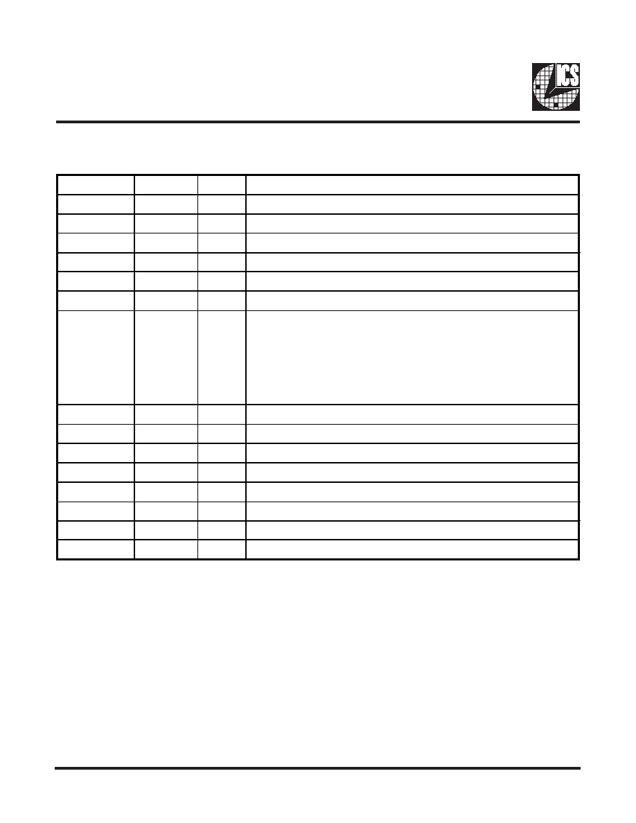
2
ICS9160-03
Preliminary Product Preview
Pin Descriptions
* Frequencies assuming an input or crystal of 14.318 MHz.
** Device provides 18pF load capacitance for crystal.
PIN NUMBER
PIN NAME
TYPE
DESCRIPTION
2X1
IN
XTAL or external reference frequency input. This input includes XTAL load
capacitance and feedback bias for a 10-30 MHz XTAL.**
3
X2
OUT
XTAL output which includes XTAL load capacitance.**
1
4
VDDX
GNDX
PWR
XTAL oscillator circuit and REFCLK output power supplies.
5, 6, 7
FS(0:2)
IN
Frequency selection address pins. These inputs have pull-ups.
8, 9, 11, 12
PCLK(0:3)
OUT
Processor clock outputs which are a multiple of the input reference frequency as
shown in the table below.
10, 17
13
VDDP
GNDP
PWR
PCLK power supplies. VDDP powers the internal PCLK PLL and the
PCLK(0:3) outputs.
14
SDATA
IN
Serial stop clock data is clocked in on the falling edge of BCLK. A total of 15 bits
must be clocked in using the following protocol. SDATA is sampled on the falling
edge of BCLK, so the data generator should change data on the rising edge of
BCLK to ensure proper communication. SDATA must be low for one BCLK period
as a start bit. The next 15 rising edges of BCLK will clock data in serially. The
16th clock enables the serial data to take effect. Outputs associated with serial data
bits that are a one will continue without interruption. Clocks associated with serial
data bits that are a zero will be stopped in the low state glitch-free, that is, no short
clocks with the exception of REFCLK and KEYBD which do not stop. This input
has an internal pull-up device.
15, 16
STOP(0:1)
IN
Stop clock control pins used for glitch-free start and stop of the clock outputs as
described in the table on the next page. These inputs have internal pull-up devices.
18
REFCLK
OUT
Buffered copy of the crystal reference frequency.
19, 21, 22, 24,
25, 27, 28
BCLK(0:6)
OUT
Bus clock outputs having selectable frequency based on the FS(0:2) inputs (see
table on next page).
20
23
GNDB
VDDB
PWR
BCLK power supplies. VSSB and VDDB power BCLK(0:6).
26
29
GNDF
VDDF
PWR
Fixed clock power supplies. VSSF and VDDF power GRAPHIC, FLOPPY and
KEYBD outputs plus the fixed clock PLL.
30
FLOPPY
OUT
The floppy clock output operates at 24 MHz..*
31
KEYBD
OUT
The keyboard clock output operates at 12 MHz.*
32
GRAPHIC
OUT
The graphics system clock output operates at 40 MHz.*
相关PDF资料 |
PDF描述 |
|---|---|
| ICS9169CF-46LF | 66.67 MHz, PROC SPECIFIC CLOCK GENERATOR, PDSO34 |
| ICS9169CF-46 | 66.67 MHz, PROC SPECIFIC CLOCK GENERATOR, PDSO34 |
| ICS9169CJ-271LF | 83.3 MHz, PROC SPECIFIC CLOCK GENERATOR, PDSO32 |
| ICS9169CJ-271 | 83.3 MHz, PROC SPECIFIC CLOCK GENERATOR, PDSO32 |
| ICS9169CM-271LF | 83.3 MHz, PROC SPECIFIC CLOCK GENERATOR, PDSO32 |
相关代理商/技术参数 |
参数描述 |
|---|---|
| ICS9161A | 制造商:ICS 制造商全称:ICS 功能描述:Dual Programmable Graphics Frequency Generator |
| ICS9161A-01CN16 | 制造商:未知厂家 制造商全称:未知厂家 功能描述:Video/Graphics Clock Generator |
| ICS9161A-01CW | 制造商:ICS 功能描述: 制造商:INT_CIR_SYS 功能描述: |
| ICS9161A-01CW16 | 功能描述:IC FREQUENCY GENERATOR 16-SOIC RoHS:否 类别:集成电路 (IC) >> 时钟/计时 - 专用 系列:- 标准包装:1,500 系列:- 类型:时钟缓冲器/驱动器 PLL:是 主要目的:- 输入:- 输出:- 电路数:- 比率 - 输入:输出:- 差分 - 输入:输出:- 频率 - 最大:- 电源电压:3.3V 工作温度:0°C ~ 70°C 安装类型:表面贴装 封装/外壳:28-SSOP(0.209",5.30mm 宽) 供应商设备封装:28-SSOP 包装:带卷 (TR) 其它名称:93786AFT |
| ICS9161A-01CW16LF | 功能描述:IC FREQUENCY GENERATOR 16-SOIC RoHS:是 类别:集成电路 (IC) >> 时钟/计时 - 专用 系列:- 标准包装:1 系列:- 类型:时钟/频率发生器,多路复用器 PLL:是 主要目的:存储器,RDRAM 输入:晶体 输出:LVCMOS 电路数:1 比率 - 输入:输出:1:2 差分 - 输入:输出:无/是 频率 - 最大:400MHz 电源电压:3 V ~ 3.6 V 工作温度:0°C ~ 85°C 安装类型:表面贴装 封装/外壳:16-TSSOP(0.173",4.40mm 宽) 供应商设备封装:16-TSSOP 包装:Digi-Reel® 其它名称:296-6719-6 |
发布紧急采购,3分钟左右您将得到回复。