- 您现在的位置:买卖IC网 > PDF目录1999 > ICS9173B-15CS08LF (IDT, Integrated Device Technology Inc)IC PLL VIDEO GENLOCK 8SOIC PDF资料下载
参数资料
| 型号: | ICS9173B-15CS08LF |
| 厂商: | IDT, Integrated Device Technology Inc |
| 文件页数: | 3/9页 |
| 文件大小: | 0K |
| 描述: | IC PLL VIDEO GENLOCK 8SOIC |
| 标准包装: | 97 |
| 类型: | 时钟/频率倍增器 |
| PLL: | 是 |
| 主要目的: | 视频同步锁相 |
| 输入: | 时钟 |
| 输出: | 时钟 |
| 电路数: | 1 |
| 比率 - 输入:输出: | 1:2 |
| 差分 - 输入:输出: | 无/无 |
| 频率 - 最大: | 37.5MHz |
| 电源电压: | 4.75 V ~ 5.25 V |
| 工作温度: | 0°C ~ 70°C |
| 安装类型: | 表面贴装 |
| 封装/外壳: | 8-SOIC(0.154",3.90mm 宽) |
| 供应商设备封装: | 8-SOIC |
| 包装: | 管件 |
ICS9173B
VIDEO GENLOCK PLL
CLOCK SYNTHESIZER
IDT VIDEO GENLOCK PLL
3
ICS9173B
REV D 012913
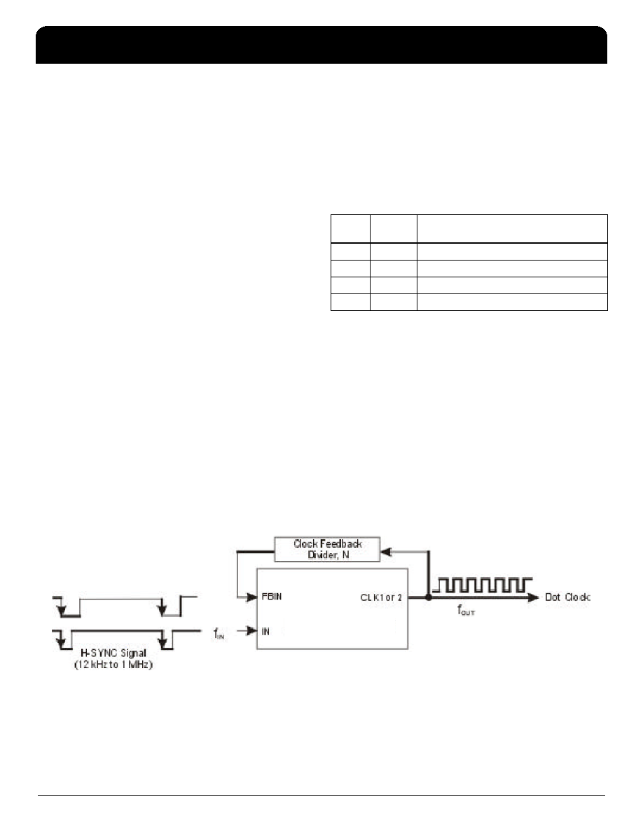
Using the ICS9173B in Genlock Applications
Most video sources, such as video cameras, are
asynchronous, free-running devices. To digitize video or
synchronize one video source to another free-running
reference video source, a video “genlock” (generator lock)
circuit is required. The ICS9173B integrates the analog
blocks which make the task much easier.
In the complete video genlock circuit, the primary function of
the ICS9173B is to provide the analog circuitry required to
generate the video dot clock within a PLL. This application
is illustrated in Figure 1. The input reference signal for this
circuit is the horizontal synchronization (H-SYNC) signal. If
a composite video reference source is being used, the
h-sync pulses must be separated from the composite signal.
A video sync separator circuit, such as the National
Semiconductor LM1881, can be used for this purpose.
The clock feedback divider shown in Figure 1 is a digital
divider used within the PLL to multiply the reference
frequency. Its divide ratio establishes how many video dot
clock cycles occur per h-sync pulse. For example, if 880
pixel clocks are desired per h-sync pulse, then the divider
ratio is set to 880. Hence, together the h-sync frequency and
external divider ratio establish the dot clock frequency:
fOUT = fIN x N where N is external divide ratio
Both input pins IN and FBIN respond only to negative-going
clock edges of the input signal. The H-SYNC signal must be
constant frequency in the 12 kHz to 1 MHz range and stable
(low clock jitter) for creation of a stable output clock.
The output hook-ups of the ICS9173B are dictated by the
desired dot clock frequency. The primary consideration is
the internal VCO which operates over a frequency range of
10 MHz to 75 MHz. Because of the selectable VCO output
divider and the additional divider on output CLK2, four
distinct output frequency ranges can be achieved. The
following Table lists these ranges and the corresponding
device configuration.
Note that both outputs, CLK1 and CLK2, are available
during operation even though only one is fed back via the
external clock divider.
Pin 5, OE, tristates both CLK1 and CLK2 upon logic low
input. This feature can be used to revert dot clock control to
the system clock when not in genlock mode (hence, when in
genlock mode the system dot clock must be tristated).
When unused, inputs FS0 and OE must be tied to either
GND (logic low) or VDD (logic high).
Figure 1: Typical Application of ICS9173B in a Video Genlock System
FS0
State
Output
Used
Frequency/Range
ICS9173B-01
Frequency/Range
IcS9173B-15
0
CLK1
10 to 75 MHz
5 to 37.5 MHz
0
CLK2
5 to 37.5 MHz
2.5 to 18.75 MHz
1
CLK1
2.5 to 18.75 MHz
1.25 to 9.375 MHz
1
CLK2
1.25 to 9.375 MHz
0.625 to 4.6875 MHz
相关PDF资料 |
PDF描述 |
|---|---|
| ICS9248BF-138LFT | IC FREQ GENERATOR/BUFFER 48-SSOP |
| ICS9250BF-12LF | IC FREQ TIMING GENERATOR 56-SSOP |
| ICS9250BF-28 | IC FREQ GENERATOR/BUFFER 56-SSOP |
| ICS9250CF-10LF | IC FREQ TIMING GENERATOR 56-SSOP |
| ICS932S200BG | IC FREQ TIMING GENERATOR 56TSSOP |
相关代理商/技术参数 |
参数描述 |
|---|---|
| ICS9173B-15CS08LFT | 功能描述:IC PLL VIDEO GENLOCK 8SOIC RoHS:是 类别:集成电路 (IC) >> 时钟/计时 - 专用 系列:- 标准包装:28 系列:- 类型:时钟/频率发生器 PLL:是 主要目的:Intel CPU 服务器 输入:时钟 输出:LVCMOS 电路数:1 比率 - 输入:输出:3:22 差分 - 输入:输出:无/是 频率 - 最大:400MHz 电源电压:3.135 V ~ 3.465 V 工作温度:0°C ~ 85°C 安装类型:表面贴装 封装/外壳:64-TFSOP (0.240",6.10mm 宽) 供应商设备封装:64-TSSOP 包装:管件 |
| ICS9175-04CN16 | 制造商:未知厂家 制造商全称:未知厂家 功能描述:CPU System Clock Generator |
| ICS9175-04CS16 | 制造商:未知厂家 制造商全称:未知厂家 功能描述:CPU System Clock Generator |
| ICS9175-04CW16 | 制造商:未知厂家 制造商全称:未知厂家 功能描述:CPU System Clock Generator |
| ICS9175-05CN16 | 制造商:未知厂家 制造商全称:未知厂家 功能描述:CPU System Clock Generator |
发布紧急采购,3分钟左右您将得到回复。