- 您现在的位置:买卖IC网 > PDF目录2075 > ICS91857AGT (IDT, Integrated Device Technology Inc)IC CLOCK DRIVER SSTL_2 48-TSSOP PDF资料下载
参数资料
| 型号: | ICS91857AGT |
| 厂商: | IDT, Integrated Device Technology Inc |
| 文件页数: | 7/14页 |
| 文件大小: | 0K |
| 描述: | IC CLOCK DRIVER SSTL_2 48-TSSOP |
| 产品变化通告: | Product Discontinuation 09/Dec/2011 |
| 标准包装: | 1,000 |
| 类型: | 时钟驱动器 |
| PLL: | 带旁路 |
| 输入: | LVCMOS |
| 输出: | SSTL-2 |
| 电路数: | 1 |
| 比率 - 输入:输出: | 1:10 |
| 差分 - 输入:输出: | 无/是 |
| 频率 - 最大: | 230MHz |
| 除法器/乘法器: | 无/无 |
| 电源电压: | 2.3 V ~ 2.7 V |
| 工作温度: | 0°C ~ 70°C |
| 安装类型: | 表面贴装 |
| 封装/外壳: | 48-TFSOP(0.240",6.10mm 宽) |
| 供应商设备封装: | 48-TSSOP |
| 包装: | 带卷 (TR) |
| 其它名称: | 91857AGT |
2
ICS91857
0494C—08/15/05
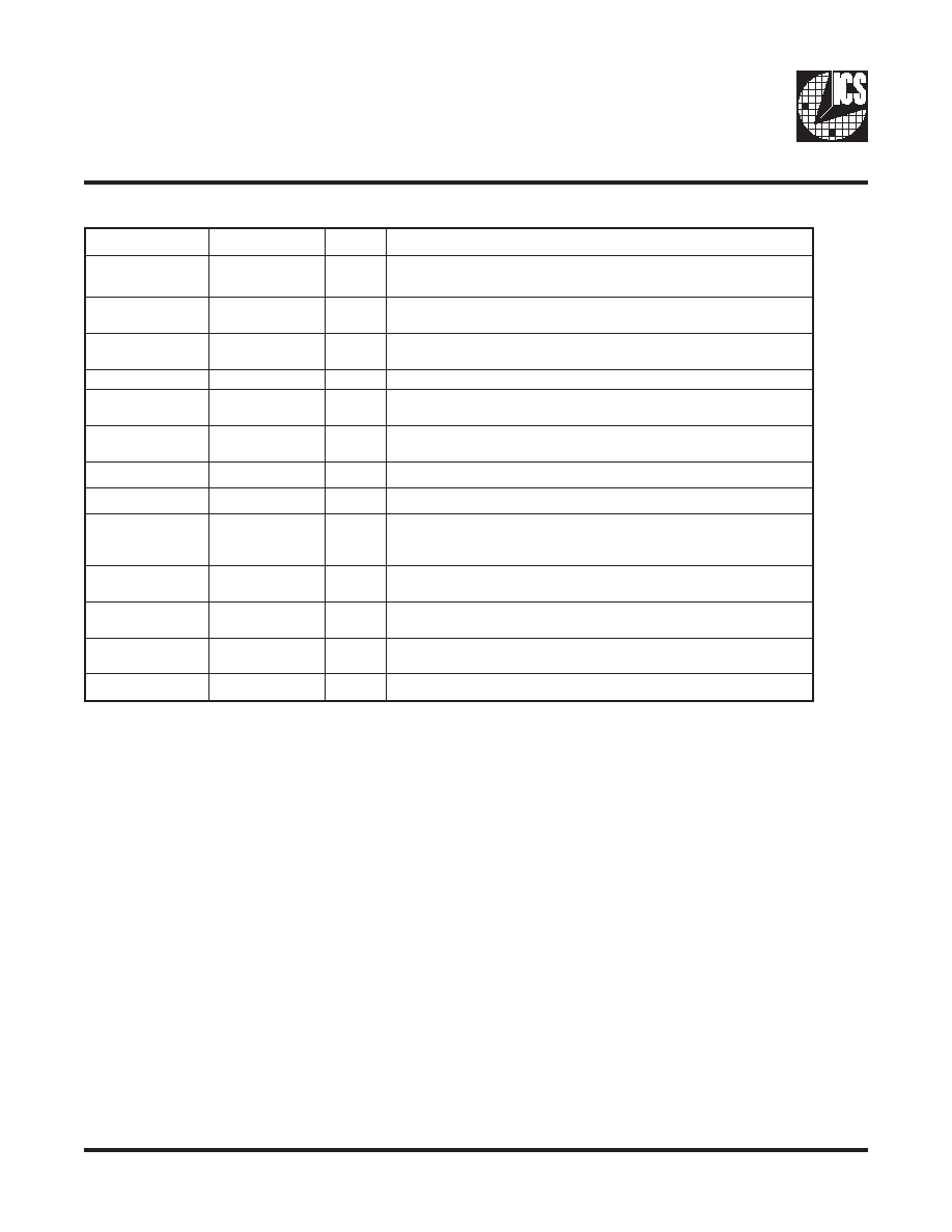
Pin Descriptions
R
E
B
M
U
N
I
PE
M
A
N
I
PE
P
Y
TN
O
I
T
P
I
R
C
S
E
D
,
1
2
,
5
1
,
2
1
,
1
,
4
,
5
4
,
8
3
,
4
3
,
8
2
D
VR
W
P
.
3
R
D
o
t
p
u
V
5
.
2
y
l
p
u
s
r
e
w
o
P
.
z
H
M
0
4
t
a
I
-
R
D
r
o
f
V
6
.
2
y
l
p
u
s
r
e
w
o
P
,
5
2
,
4
2
,
8
1
,
8
,
7
,
1
8
4
,
2
4
,
1
4
,
1
3
D
N
GR
W
Pd
n
u
o
r
G
6
1D
D
V
AR
W
P
.
3
R
D
o
t
p
u
V
5
.
2
,
y
l
p
u
s
r
e
w
o
p
g
o
l
a
n
A
.
z
H
M
0
4
t
a
I
-
R
D
r
o
f
V
6
.
2
y
l
p
u
s
r
e
w
o
P
7
1D
N
G
AR
W
P.
d
n
u
o
r
g
o
l
a
n
A
,
6
4
,
4
,
9
3
,
9
2
,
7
2
3
,
5
,
0
1
,
0
2
,
2
)
0
:
9
(
T
K
L
CT
U
O.
s
t
u
p
t
u
o
r
i
a
p
l
a
i
t
n
e
r
e
f
i
d
f
o
k
c
o
l
C
"
e
u
r
T
"
,
7
4
,
3
4
,
0
4
,
0
3
,
6
2
,
6
,
9
,
9
1
,
3
2
)
0
:
9
(
C
K
L
CT
U
O.
s
t
u
p
t
u
o
r
i
a
p
l
a
i
t
n
e
r
e
f
i
d
f
o
s
k
c
o
l
c
"
y
r
a
t
n
e
m
e
l
p
m
o
C
"
4
1C
N
I
_
K
L
CN
It
u
p
n
i
k
c
o
l
c
e
c
n
e
r
e
f
e
r
"
y
r
a
t
n
e
m
e
l
p
m
o
C
"
3
1T
N
I
_
K
L
CN
It
u
p
n
i
k
c
o
l
c
e
c
n
e
r
e
f
e
r
"
e
u
r
T
"
3
3C
T
U
O
_
B
FT
U
O
t
I
.
k
c
a
b
d
e
f
l
a
n
r
e
t
x
e
r
o
f
d
e
t
a
c
i
d
e
d
,
t
u
p
t
u
o
k
c
a
b
d
e
F
"
y
r
a
t
n
e
m
e
l
p
m
o
C
"
d
e
r
i
w
e
b
t
s
u
m
t
u
p
t
u
o
s
i
h
T
.
K
L
C
e
h
t
s
a
y
c
n
e
u
q
e
r
f
e
m
a
s
e
h
t
a
s
e
h
c
t
i
w
s
.
C
N
I
_
B
F
o
t
2
3T
T
U
O
_
B
FT
U
O
t
a
s
e
h
c
t
i
w
s
t
I
.
k
c
a
b
d
e
f
l
a
n
r
e
t
x
e
r
o
f
d
e
t
a
c
i
d
e
d
,
t
u
p
t
u
o
k
c
a
b
d
e
F
"
e
u
r
T
"
.
T
N
I
_
B
F
o
t
d
e
r
i
w
e
b
t
s
u
m
t
u
p
t
u
o
s
i
h
T
.
K
L
C
e
h
t
s
a
y
c
n
e
u
q
e
r
f
e
m
a
s
e
h
t
6
3T
N
I
_
B
FN
I
r
o
f
L
P
l
a
n
r
e
t
n
i
e
h
t
o
t
l
a
n
g
i
s
k
c
a
b
d
e
f
s
e
d
i
v
o
r
p
,
t
u
p
n
i
k
c
a
b
d
e
F
"
e
u
r
T
"
.
r
o
r
e
s
a
h
p
e
t
a
n
i
m
il
e
o
t
T
N
I
_
K
L
C
h
t
i
w
n
o
i
t
a
z
i
n
o
r
h
c
n
y
s
5
3C
N
I
_
B
FN
I
L
P
l
a
n
r
e
t
n
i
e
h
t
o
t
l
a
n
g
i
s
e
d
i
v
o
r
p
,
t
u
p
n
i
k
c
a
b
d
e
F
"
y
r
a
t
n
e
m
e
l
p
m
o
C
"
.
r
o
r
e
s
a
h
p
e
t
a
n
i
m
il
e
o
t
C
N
I
_
K
L
C
h
t
i
w
n
o
i
t
a
z
i
n
o
r
h
c
n
y
s
r
o
f
7
3#
D
PN
It
u
p
n
i
S
O
M
C
V
L
.
n
w
o
D
r
e
w
o
P
This PLL Clock Buffer is designed for a VDD of 2.5V, an AVDD of 2.5V and differential data input and output levels.
ICS91857 is a zero delay buffer that distributes a differential clock input pair (CLK_INC, CLK_INT) to ten differential
pair of clock outputs (CLKT[0:9], CLKC[0:9]) and one differential pair feedback clock output (FB_OUT, FB_OUTC).The
clock outputs are controlled by the input clocks (CLK_INC, CLK_INT), the feedback clocks (FB_INT, FB_INC) the 2.5-
V LVCMOS input (PD#) and the Analog Power input (AVDD).When input (PD#) is low while power is applied, the receivers
are disabled, the PLL is turned off and the differential clock outputs are Tri-Stated. When AVDD is grounded, the PLL
is turned off and bypassed for test purposes.
When the input frequency is less than the operating frequency of the PLL, appproximately 20MHz, the device will
enter a low power mode. An input frequency detection circuit on the differential inputs, independent from the input
buffers, will detect the low frequency condition and perform the same low power features as when the (PD#) input
is low. When the input frequency increases to greater than approximately 20 MHz, the PLL will be turned back on,
the inputs and outputs will be enabled and PLL will obtain phase lock between the feedback clock pair (FB_INT,
FB_INC) and the input clock pair (CLK_INC, CLK_INT).
The PLL in the ICS91857 clock driver uses the input clocks (CLK_INC, CLK_INT) and the feedback clocks (FB_INT,
FB_INC) provide high-performance, low-skew, low-jitter output differential clocks (CLKT [0:9], CLKC [0:9]). The
ICS91857 is also able to track Spread Spectrum Clock (SSC) for reduced EMI.
ICS91857 is characterized for operation from 0°C to 70°C and will meet JEDEC Standard 82-1 and 82-1A for Registered
DDR Clock Driver.
相关PDF资料 |
PDF描述 |
|---|---|
| ICS93718CFLFT | IC CLK BUFF 2:12 200MHZ 48-SSOP |
| ICS951601AFLFT | IC FREQ TIMING GENERATOR 48-SSOP |
| ICS95V157AGIT | IC CLK BUFF 1:10 233MHZ 48-TSSOP |
| ICS97U877AKT | IC CLK DVR PLL 1:10 40VFQFN |
| ICS9DS400AGLF | IC CLK SPREAD INJECTION 28TSSOP |
相关代理商/技术参数 |
参数描述 |
|---|---|
| ICS91857YGLFT-LF-T | 制造商:ICS 制造商全称:ICS 功能描述:Value SSTL_2 Clock Driver (60MHz - 220MHz) |
| ICS91857YLLFT-LF-T | 制造商:ICS 制造商全称:ICS 功能描述:Value SSTL_2 Clock Driver (60MHz - 220MHz) |
| ICS9212-13 | 制造商:ICS 制造商全称:ICS 功能描述:Direct Rambus⑩ Clock Generator |
| ICS9212AF-13 | 功能描述:IC CLK GEN DIRECT RAMBUS 24-SSOP RoHS:否 类别:集成电路 (IC) >> 时钟/计时 - 专用 系列:- 标准包装:28 系列:- 类型:时钟/频率发生器 PLL:是 主要目的:Intel CPU 服务器 输入:时钟 输出:LVCMOS 电路数:1 比率 - 输入:输出:3:22 差分 - 输入:输出:无/是 频率 - 最大:400MHz 电源电压:3.135 V ~ 3.465 V 工作温度:0°C ~ 85°C 安装类型:表面贴装 封装/外壳:64-TFSOP (0.240",6.10mm 宽) 供应商设备封装:64-TSSOP 包装:管件 |
| ICS9212AF-13LF | 功能描述:IC CLK GEN DIRECT RAMBUS 24-SSOP RoHS:是 类别:集成电路 (IC) >> 时钟/计时 - 专用 系列:- 标准包装:28 系列:- 类型:时钟/频率发生器 PLL:是 主要目的:Intel CPU 服务器 输入:时钟 输出:LVCMOS 电路数:1 比率 - 输入:输出:3:22 差分 - 输入:输出:无/是 频率 - 最大:400MHz 电源电压:3.135 V ~ 3.465 V 工作温度:0°C ~ 85°C 安装类型:表面贴装 封装/外壳:64-TFSOP (0.240",6.10mm 宽) 供应商设备封装:64-TSSOP 包装:管件 |
发布紧急采购,3分钟左右您将得到回复。