- 您现在的位置:买卖IC网 > PDF目录79599 > ICS94228BFT (INTEGRATED DEVICE TECHNOLOGY INC) 233.33 MHz, PROC SPECIFIC CLOCK GENERATOR, PDSO48 PDF资料下载
参数资料
| 型号: | ICS94228BFT |
| 厂商: | INTEGRATED DEVICE TECHNOLOGY INC |
| 元件分类: | 时钟产生/分配 |
| 英文描述: | 233.33 MHz, PROC SPECIFIC CLOCK GENERATOR, PDSO48 |
| 封装: | 0.300 INCH, MO-118, SSOP-48 |
| 文件页数: | 8/19页 |
| 文件大小: | 189K |
| 代理商: | ICS94228BFT |
16
ICS94228
0447E—05/07/04
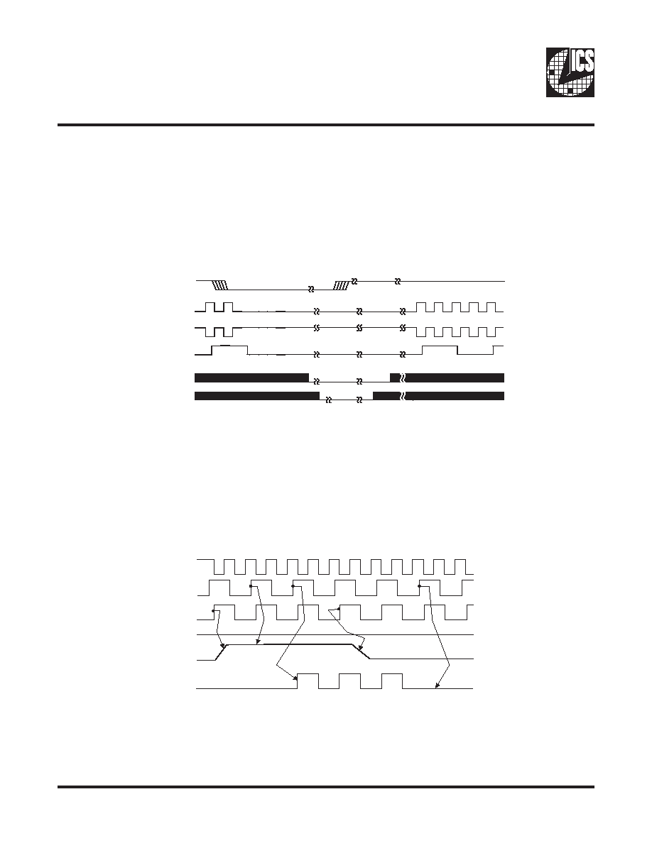
PD# Timing Diagram
The power down selection is used to put the part into a very low power state without turning off the power to the part.
PD# is an asynchronous active low input. This signal needs to be synchronized internal to the device prior to powering
down the clock synthesizer.
Internal clocks are not running after the device is put in power down. When PD# is active low all clocks need to be driven
to a low value and held prior to turning off the VCOs and crystal. The power up latency needs to be less than 3 mS.
The power down latency should be as short as possible but conforming to the sequence requirements shown below.
PCI_STOP# and CPU_STOP# are considered to be don't cares during the power down operations. The REF and 48MHz
clocks are expected to be stopped in the LOW state as soon as possible. Due to the state of the internal logic, stopping
and holding the REF clock outputs in the LOW state may require more than one clock cycle to complete.
Notes:
1. All timing is referenced to the Internal CPUCLK (defined as inside the ICS94228 device).
2. As shown, the outputs Stop Low on the next falling edge after PD# goes low.
3. PD# is an asynchronous input and metastable conditions may exist. This signal is synchronized inside this part.
4. The shaded sections on the VCO and the Crystal signals indicate an active clock.
5. Diagrams shown with respect to 133MHz. Similar operation when CPU is 100MHz.
CPUCLKT
CPUCLKC
PCICLK
VCO
Crystal
PD#
PCI_STOP# Timing Diagram
PCI_STOP# is an asynchronous input to the ICS94228. It is used to turn off the PCICLK clocks for low power operation.
PCI_STOP# is synchronized by the ICS94228 internally. The minimum that the PCICLK clocks are enabled
(PCI_STOP# high pulse) is at least 10 PCICLK clocks. PCICLK clocks are stopped in a low state and started with a
full high pulse width guaranteed. PCICLK clock on latency cycles are only one rising PCICLK clock off latency is one
PCICLK clock.
Notes:
1. All timing is referenced to the Internal CPUCLK (defined as inside the ICS94228 device.)
2. PCI_STOP# is an asynchronous input, and metastable conditions may exist. This signal is required to be synchronized
inside the ICS94228.
3. All other clocks continue to run undisturbed.
4. CPU_STOP# is shown in a high (true) state.
CPUCLK
(Internal)
PCICLK_F
(Internal)
PCICLK_F
(Free-running)
CPU_STOP#
PCICLK
PCI_STOP#
相关PDF资料 |
PDF描述 |
|---|---|
| ICS952302AGT | PROC SPECIFIC CLOCK GENERATOR, PDSO48 |
| IS80C51C-L16R | 8-BIT, MROM, 16 MHz, MICROCONTROLLER, PQCC44 |
| IF280C51-25D | 8-BIT, MROM, 25 MHz, MICROCONTROLLER, PQFP44 |
| IP80C51T-25D | 8-BIT, MROM, 25 MHz, MICROCONTROLLER, PDIP40 |
| IS80C51T-20R | 8-BIT, MROM, 20 MHz, MICROCONTROLLER, PQCC44 |
相关代理商/技术参数 |
参数描述 |
|---|---|
| ICS94228YFLF-T | 制造商:ICS 制造商全称:ICS 功能描述:Programmable System Clock Chip for AMD - K7⑩ processor |
| ICS94229 | 制造商:ICS 制造商全称:ICS 功能描述:Programmable System Clock Chip for AMD - K7 processor |
| ICS94229YF-T | 制造商:ICS 制造商全称:ICS 功能描述:Programmable System Clock Chip for AMD - K7 processor |
| ICS94230BF | 功能描述:IC CLOCK CHIP PROGR AMDK7 48SSOP RoHS:否 类别:集成电路 (IC) >> 时钟/计时 - 专用 系列:- 标准包装:1,500 系列:- 类型:时钟缓冲器/驱动器 PLL:是 主要目的:- 输入:- 输出:- 电路数:- 比率 - 输入:输出:- 差分 - 输入:输出:- 频率 - 最大:- 电源电压:3.3V 工作温度:0°C ~ 70°C 安装类型:表面贴装 封装/外壳:28-SSOP(0.209",5.30mm 宽) 供应商设备封装:28-SSOP 包装:带卷 (TR) 其它名称:93786AFT |
| ICS94230BFLF | 功能描述:IC CLOCK CHIP PROGR AMDK7 48SSOP RoHS:是 类别:集成电路 (IC) >> 时钟/计时 - 专用 系列:- 标准包装:28 系列:- 类型:时钟/频率发生器 PLL:是 主要目的:Intel CPU 服务器 输入:时钟 输出:LVCMOS 电路数:1 比率 - 输入:输出:3:22 差分 - 输入:输出:无/是 频率 - 最大:400MHz 电源电压:3.135 V ~ 3.465 V 工作温度:0°C ~ 85°C 安装类型:表面贴装 封装/外壳:64-TFSOP (0.240",6.10mm 宽) 供应商设备封装:64-TSSOP 包装:管件 |
发布紧急采购,3分钟左右您将得到回复。