- 您现在的位置:买卖IC网 > PDF目录67709 > ICS9DB108YFT (INTEGRATED DEVICE TECHNOLOGY INC) 9DB SERIES, PLL BASED CLOCK DRIVER, 8 TRUE OUTPUT(S), 0 INVERTED OUTPUT(S), PDSO48 PDF资料下载
参数资料
| 型号: | ICS9DB108YFT |
| 厂商: | INTEGRATED DEVICE TECHNOLOGY INC |
| 元件分类: | 时钟及定时 |
| 英文描述: | 9DB SERIES, PLL BASED CLOCK DRIVER, 8 TRUE OUTPUT(S), 0 INVERTED OUTPUT(S), PDSO48 |
| 封装: | MO-118, SSOP-48 |
| 文件页数: | 3/16页 |
| 文件大小: | 140K |
| 代理商: | ICS9DB108YFT |
11
Integrated
Circuit
Systems, Inc.
ICS9DB108
0723E—10/26/05
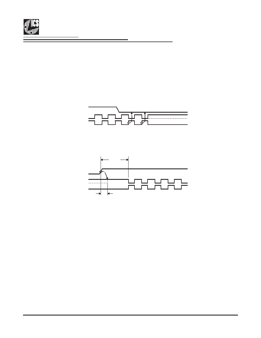
The PD# pin cleanly shuts off all clocks and places the device into a power saving mode. PD# must be asserted before
shutting off the input clock or power to insure an orderly shutdown. PD is asynchronous active-low input for both powering
down the device and powering up the device. When PD# is asserted, all clocks will be driven high, or tri-stated (depending
on the PD# drive mode and Output control bits) before the PLL is shut down.
PD#, Power Down
When PD# is sampled low by two consecutive rising edges of DIF#, all DIF outputs must be held High, or tri-stated (depending
on the PD# drive mode and Output control bits) on the next High-Low transition of the DIF# outputs. When the PD# drive mode
bit is set to ‘0’, all clock outputs will be held with DIF driven High with 2 x IREF and DIF# tri-stated. If the PD# drive mode bit is
set to ‘1’, both DIF and DIF# are tri-stated.
PD# Assertion
Power-up latency is less than 1 ms. This is the time from de-assertion of the PD# pin, or VDD reaching 3.3V, or the time from
valid SRC_IN clocks until the time that stable clocks are output from the device (PLL Locked). If the PD# drive mode bit is set
to ‘1’, all the DIF outputs must driven to a voltage of >200 mV within 300 ms of PD# de-assertion.
PD# De-assertion
PWRDWN#
DIF
DIF#
PWRDWN#
DIF
DIF#
Tstable
<1mS
Tdrive_PwrDwn#
<300uS, >200mV
相关PDF资料 |
PDF描述 |
|---|---|
| ICS9DB108YGT | 9DB SERIES, PLL BASED CLOCK DRIVER, 8 TRUE OUTPUT(S), 0 INVERTED OUTPUT(S), PDSO48 |
| ICS9DB108YGLFT | 9DB SERIES, PLL BASED CLOCK DRIVER, 8 TRUE OUTPUT(S), 0 INVERTED OUTPUT(S), PDSO48 |
| ICS9DB202CF | 9DB SERIES, PLL BASED CLOCK DRIVER, 2 TRUE OUTPUT(S), 0 INVERTED OUTPUT(S), PDSO20 |
| ICS9DB206CLLFT | 9DB SERIES, PLL BASED CLOCK DRIVER, 6 TRUE OUTPUT(S), 0 INVERTED OUTPUT(S), PDSO28 |
| ICS9DB206CFT | 9DB SERIES, PLL BASED CLOCK DRIVER, 6 TRUE OUTPUT(S), 0 INVERTED OUTPUT(S), PDSO28 |
相关代理商/技术参数 |
参数描述 |
|---|---|
| ICS9DB1200CGLF | 功能描述:IC BUFFER 12OUTPUT DIFF 64TSSOP RoHS:是 类别:集成电路 (IC) >> 时钟/计时 - 专用 系列:PCI Express® (PCIe) 标准包装:1 系列:- 类型:时钟/频率发生器,多路复用器 PLL:是 主要目的:存储器,RDRAM 输入:晶体 输出:LVCMOS 电路数:1 比率 - 输入:输出:1:2 差分 - 输入:输出:无/是 频率 - 最大:400MHz 电源电压:3 V ~ 3.6 V 工作温度:0°C ~ 85°C 安装类型:表面贴装 封装/外壳:16-TSSOP(0.173",4.40mm 宽) 供应商设备封装:16-TSSOP 包装:Digi-Reel® 其它名称:296-6719-6 |
| ICS9DB1200CGLFT | 功能描述:IC BUFFER 12OUTPUT DIFF 64-TSSOP RoHS:是 类别:集成电路 (IC) >> 时钟/计时 - 专用 系列:PCI Express® (PCIe) 标准包装:1 系列:- 类型:时钟/频率发生器,多路复用器 PLL:是 主要目的:存储器,RDRAM 输入:晶体 输出:LVCMOS 电路数:1 比率 - 输入:输出:1:2 差分 - 输入:输出:无/是 频率 - 最大:400MHz 电源电压:3 V ~ 3.6 V 工作温度:0°C ~ 85°C 安装类型:表面贴装 封装/外壳:16-TSSOP(0.173",4.40mm 宽) 供应商设备封装:16-TSSOP 包装:Digi-Reel® 其它名称:296-6719-6 |
| ICS9DB1233AGLF | 功能描述:IC CLK FANOUT/BUFF ZD 64TSSOP RoHS:是 类别:集成电路 (IC) >> 时钟/计时 - 专用 系列:PCI Express® (PCIe) 标准包装:28 系列:- 类型:时钟/频率发生器 PLL:是 主要目的:Intel CPU 服务器 输入:时钟 输出:LVCMOS 电路数:1 比率 - 输入:输出:3:22 差分 - 输入:输出:无/是 频率 - 最大:400MHz 电源电压:3.135 V ~ 3.465 V 工作温度:0°C ~ 85°C 安装类型:表面贴装 封装/外壳:64-TFSOP (0.240",6.10mm 宽) 供应商设备封装:64-TSSOP 包装:管件 |
| ICS9DB1233AGLFT | 功能描述:IC CLK FANOUT/BUFF ZD 64TSSOP RoHS:否 类别:集成电路 (IC) >> 时钟/计时 - 专用 系列:PCI Express® (PCIe) 标准包装:28 系列:- 类型:时钟/频率发生器 PLL:是 主要目的:Intel CPU 服务器 输入:时钟 输出:LVCMOS 电路数:1 比率 - 输入:输出:3:22 差分 - 输入:输出:无/是 频率 - 最大:400MHz 电源电压:3.135 V ~ 3.465 V 工作温度:0°C ~ 85°C 安装类型:表面贴装 封装/外壳:64-TFSOP (0.240",6.10mm 宽) 供应商设备封装:64-TSSOP 包装:管件 |
| ICS9DB1904BKLF | 功能描述:IC CLK FANOUT/BUFF ZD 72VFQFN RoHS:是 类别:集成电路 (IC) >> 时钟/计时 - 专用 系列:PCI Express® (PCIe) 标准包装:28 系列:- 类型:时钟/频率发生器 PLL:是 主要目的:Intel CPU 服务器 输入:时钟 输出:LVCMOS 电路数:1 比率 - 输入:输出:3:22 差分 - 输入:输出:无/是 频率 - 最大:400MHz 电源电压:3.135 V ~ 3.465 V 工作温度:0°C ~ 85°C 安装类型:表面贴装 封装/外壳:64-TFSOP (0.240",6.10mm 宽) 供应商设备封装:64-TSSOP 包装:管件 |
发布紧急采购,3分钟左右您将得到回复。