- 您现在的位置:买卖IC网 > PDF目录1999 > ICS9DB202CFLF (IDT, Integrated Device Technology Inc)IC JITTER ATTENUATOR 20-SSOP PDF资料下载
参数资料
| 型号: | ICS9DB202CFLF |
| 厂商: | IDT, Integrated Device Technology Inc |
| 文件页数: | 5/13页 |
| 文件大小: | 0K |
| 描述: | IC JITTER ATTENUATOR 20-SSOP |
| 标准包装: | 64 |
| 系列: | HiPerClockS™, PCI Express® (PCIe) |
| 类型: | 漂移衰减器,多路复用器 |
| PLL: | 是 |
| 主要目的: | PCI Express(PCIe) |
| 输入: | HCSL,LVDS,LVHSTL,LVPECL,SSTL |
| 输出: | HCSL |
| 电路数: | 1 |
| 比率 - 输入:输出: | 1:2 |
| 差分 - 输入:输出: | 是/是 |
| 频率 - 最大: | 140MHz |
| 电源电压: | 3.135 V ~ 3.465 V |
| 工作温度: | 0°C ~ 70°C |
| 安装类型: | 表面贴装 |
| 封装/外壳: | 20-SSOP(0.209",5.30mm 宽) |
| 供应商设备封装: | 20-SSOP |
| 包装: | 管件 |
| 其它名称: | 9DB202CFLF |
CS5532/34-BS
DS755F3
13
instrumentation amplifier is typically 1200 pA
over
-40°C to +85°C (MCLK=4.9152 MHz).
The common-mode plus signal range of the instru-
mentation amplifier is (VA-) + 0.7 V to (VA+) -
1.7 V.
Figure 4 illustrates the input models for the ampli-
fiers. The dynamic input current for each of the
pins can be determined from the models shown.
Note:
The C=3.9pF and C = 14pF capacitors are
for input current modeling only. For physical
input capacitance see ‘Input Capacitance’
specification under Analog Characteristics.
2.1.1. Analog Input Span
The full-scale input signal that the converter can
digitize is a function of the gain setting and the ref-
erence voltage connected between the VREF+ and
VREF- pins. The full-scale input span of the con-
verter is ((VREF+) - (VREF-))/(GxA), where G is
the gain of the amplifier and A is 2 for VRS = 0, or
A is 1 for VRS = 1. VRS is the Voltage Reference
Select bit, and must be set according to the differen-
tial voltage applied to the VREF+ and VREF- pins
on the part. See section 2.3.5 for more details.
After reset, the unity gain buffer is engaged. With a
2.5 V reference this would make the full-scale input
range default to 2.5 V. By activating the instrumen-
tation amplifier (i.e. a gain setting other than 1) and
using a gain setting of 32, the full-scale input range
can quickly be set to 2.5/32 or about 78 mV. Note
that these input ranges assume the calibration regis-
ters are set to their default values (i.e. Gain = 1.0 and
Offset = 0.0).
2.1.2. Multiplexed Settling Limitations
The settling performance of the CS5532/34 in mul-
tiplexed applications is affected by the single-pole,
low-pass filter which follows the instrumentation
amplifier (see Figure 3). To achieve data sheet set-
tling and linearity specifications, it is recommend-
ed that a 22 nF C0G capacitor be used. Capacitors
as low as 10 nF or X7R type capacitors can also be
used with some minor increase in distortion for AC
signals.
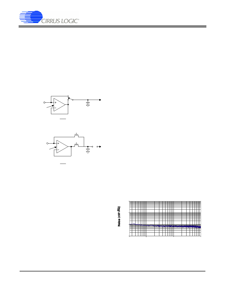
2.1.3. Voltage Noise Density Performance
Figure 5 illustrates the measured voltage noise
density versus frequency from 0.025 Hz to 10 Hz
of a CS5532-BS. The device was powered with
±2.5 V supplies, using 30 Sps OWR, the 64x gain
range, bipolar mode, and with the input short bit
enabled.
AIN
Gain =2, 4,8,16, 32,64
C =3 .9 pF
f=
Gain = 1
AIN
C= 14 pF
φ Coarse
1
φ Fine
1
V
≤ 12 mV
i= fV
C
os
n
V
≤ 8mV
i= fV
C
os
n
MCLK
128
f=
MCLK
16
Figure 4. Input models for AIN+ and AIN- pins
1
10
100
1000
0.025
0.10
1.00
10.00
Frequency (Hz)
Figure 5. Measured Voltage Noise Density, 64x
相关PDF资料 |
PDF描述 |
|---|---|
| ICS9DB202CK-01LFT | IC JITTER ATTENUATOR 32-VFQFPN |
| ICS9DB206CLLF | IC JITTER ATTENUATOR 28-TSSOP |
| ICS9DB306BLLFT | IC JITTER ATTENUATOR 28-TSSOP |
| ICS9E4101AFILFT | IC TIMING CTRL HUB PROG 56SSOP |
| ICS9EX21801AKLF | IC FANOUT BUFF DIFF 72-VFQFN |
相关代理商/技术参数 |
参数描述 |
|---|---|
| ICS9DB202CFLFT | 功能描述:IC JITTER ATTENUATOR 20-SSOP RoHS:是 类别:集成电路 (IC) >> 时钟/计时 - 专用 系列:HiPerClockS™, PCI Express® (PCIe) 标准包装:1,500 系列:- 类型:时钟缓冲器/驱动器 PLL:是 主要目的:- 输入:- 输出:- 电路数:- 比率 - 输入:输出:- 差分 - 输入:输出:- 频率 - 最大:- 电源电压:3.3V 工作温度:0°C ~ 70°C 安装类型:表面贴装 封装/外壳:28-SSOP(0.209",5.30mm 宽) 供应商设备封装:28-SSOP 包装:带卷 (TR) 其它名称:93786AFT |
| ICS9DB202CGLF | 功能描述:IC JITTER ATTENUATOR 20-TSSOP RoHS:是 类别:集成电路 (IC) >> 时钟/计时 - 专用 系列:HiPerClockS™, PCI Express® (PCIe) 标准包装:1 系列:- 类型:时钟/频率发生器,多路复用器 PLL:是 主要目的:存储器,RDRAM 输入:晶体 输出:LVCMOS 电路数:1 比率 - 输入:输出:1:2 差分 - 输入:输出:无/是 频率 - 最大:400MHz 电源电压:3 V ~ 3.6 V 工作温度:0°C ~ 85°C 安装类型:表面贴装 封装/外壳:16-TSSOP(0.173",4.40mm 宽) 供应商设备封装:16-TSSOP 包装:Digi-Reel® 其它名称:296-6719-6 |
| ICS9DB202CGLFT | 功能描述:IC JITTER ATTENUATOR 20-TSSOP RoHS:是 类别:集成电路 (IC) >> 时钟/计时 - 专用 系列:HiPerClockS™, PCI Express® (PCIe) 标准包装:1,500 系列:- 类型:时钟缓冲器/驱动器 PLL:是 主要目的:- 输入:- 输出:- 电路数:- 比率 - 输入:输出:- 差分 - 输入:输出:- 频率 - 最大:- 电源电压:3.3V 工作温度:0°C ~ 70°C 安装类型:表面贴装 封装/外壳:28-SSOP(0.209",5.30mm 宽) 供应商设备封装:28-SSOP 包装:带卷 (TR) 其它名称:93786AFT |
| ICS9DB202CK-01LF | 功能描述:IC JITTER ATTENUATOR 32-VFQFN RoHS:是 类别:集成电路 (IC) >> 时钟/计时 - 专用 系列:HiPerClockS™, PCI Express® (PCIe) 标准包装:1 系列:- 类型:时钟/频率发生器,多路复用器 PLL:是 主要目的:存储器,RDRAM 输入:晶体 输出:LVCMOS 电路数:1 比率 - 输入:输出:1:2 差分 - 输入:输出:无/是 频率 - 最大:400MHz 电源电压:3 V ~ 3.6 V 工作温度:0°C ~ 85°C 安装类型:表面贴装 封装/外壳:16-TSSOP(0.173",4.40mm 宽) 供应商设备封装:16-TSSOP 包装:Digi-Reel® 其它名称:296-6719-6 |
| ICS9DB202CK-01LFT | 功能描述:IC JITTER ATTENUATOR 32-VFQFPN RoHS:是 类别:集成电路 (IC) >> 时钟/计时 - 专用 系列:HiPerClockS™, PCI Express® (PCIe) 标准包装:1,500 系列:- 类型:时钟缓冲器/驱动器 PLL:是 主要目的:- 输入:- 输出:- 电路数:- 比率 - 输入:输出:- 差分 - 输入:输出:- 频率 - 最大:- 电源电压:3.3V 工作温度:0°C ~ 70°C 安装类型:表面贴装 封装/外壳:28-SSOP(0.209",5.30mm 宽) 供应商设备封装:28-SSOP 包装:带卷 (TR) 其它名称:93786AFT |
发布紧急采购,3分钟左右您将得到回复。