- 您现在的位置:买卖IC网 > PDF目录9591 > ICS9DB202CFLFT (IDT, Integrated Device Technology Inc)IC JITTER ATTENUATOR 20-SSOP PDF资料下载
参数资料
| 型号: | ICS9DB202CFLFT |
| 厂商: | IDT, Integrated Device Technology Inc |
| 文件页数: | 4/13页 |
| 文件大小: | 0K |
| 描述: | IC JITTER ATTENUATOR 20-SSOP |
| 标准包装: | 1,000 |
| 系列: | HiPerClockS™, PCI Express® (PCIe) |
| 类型: | 漂移衰减器,多路复用器 |
| PLL: | 是 |
| 主要目的: | PCI Express(PCIe) |
| 输入: | HCSL,LVDS,LVHSTL,LVPECL,SSTL |
| 输出: | HCSL |
| 电路数: | 1 |
| 比率 - 输入:输出: | 1:2 |
| 差分 - 输入:输出: | 是/是 |
| 频率 - 最大: | 140MHz |
| 电源电压: | 3.135 V ~ 3.465 V |
| 工作温度: | 0°C ~ 70°C |
| 安装类型: | 表面贴装 |
| 封装/外壳: | 20-SSOP(0.209",5.30mm 宽) |
| 供应商设备封装: | 20-SSOP |
| 包装: | 带卷 (TR) |
| 其它名称: | 9DB202CFLFT |
CS5532/34-BS
12
DS755F3
2. GENERAL DESCRIPTION
The CS5532/34 are highly integrated
Σ Analog-
to-Digital Converters (ADCs) which use charge-
balance techniques to achieve 24-bit performance.
The ADCs are optimized for measuring low-level
unipolar or bipolar signals in weigh scale, process
control, scientific, and medical applications.
To accommodate these applications, the ADCs
come as either two-channel (CS5532) or four-chan-
nel (CS5534) devices and include a very-low-
noise, chopper-stabilized, programmable-gain in-
strumentation amplifier (PGIA, 6 nV/
√Hz @
0.1 Hz) with selectable gains of 1×, 2×, 4×, 8×,
16×, 32×, and 64×. These ADCs also include a
fourth-order
Σ modulator followed by a digital
filter which provides twenty selectable output word
rates of 6.25, 7.5, 12.5, 15, 25, 30, 50, 60, 100, 120,
200, 240, 400, 480, 800, 960, 1600, 1920, 3200, and
3840 Samples per second (MCLK = 4.9152 MHz).
To ease communication between the ADCs and a
microcontroller, the converters include a simple
three-wire serial interface which is SPI and Mi-
crowire compatible with a Schmitt-trigger input on
the serial clock (SCLK).
2.1. Analog Input
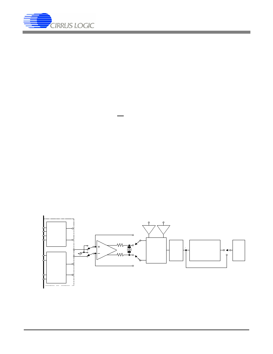
Figure 3 illustrates a block diagram of the
CS5532/34. The front end consists of a multiplexer,
a unity gain coarse/fine charge input buffer, and a
programmable-gain, chopper-stabilized instrumen-
tation amplifier. The unity gain buffer is activated
any time conversions are performed with a gain of
one and the instrumentation amplifier is activated
any time conversions are performed with gain set-
tings greater than one.
The unity gain buffer is designed to accommodate
rail-to-rail input signals. The common mode plus
signal range for the unity gain buffer amplifier is
VA- to VA+. Typical CVF (sampling) current for
the unity gain buffer amplifier is about 50 nA
(MCLK = 4.9152 MHz, see Figure 4).
The instrumentation amplifier is chopper stabilized
and operates with a chop-clock frequency of
MCLK/128. The CVF (sampling) current into the
VREF+
Sinc
Digital
Filter
XGAIN
M
U
X
AIN2+
AIN2-
AIN1+
AIN1-
CS5531/32 IN+
IN-
AIN4+
AIN4-
*
AIN1+
AIN1-
CS5533/34
M
U
X
IN+
IN-
IN+
IN-
GAIN is the gain setting of the PGIA (i.e. 2, 4, 8, 16, 32, 64)
X1
VREF-
X1
Differential
4
Order
Σ
Modulator
th
5
Programmable
Sinc
Digital Filter
3
Serial
Port
1000
1000
22 nF
C1 PIN
C2 PIN
X1
Figure 3. Multiplexer Configuration
相关PDF资料 |
PDF描述 |
|---|---|
| MS3128F16-26P | CONN RCPT 26POS WALL MNT W/PINS |
| MS3128F14-12S | CONN RCPT 12POS WALL MNT W/SCKT |
| SL28504BZI-2T | IC CLOCK GEN EAGLELAKE 56TSSOP |
| ICL3238CA-T | IC 5DRVR/3RCVR RS232 3V 28-SSOP |
| ICL3238CA | IC 5DRVR/3RCVR RS232 3V 28-SSOP |
相关代理商/技术参数 |
参数描述 |
|---|---|
| ICS9DB202CGLF | 功能描述:IC JITTER ATTENUATOR 20-TSSOP RoHS:是 类别:集成电路 (IC) >> 时钟/计时 - 专用 系列:HiPerClockS™, PCI Express® (PCIe) 标准包装:1 系列:- 类型:时钟/频率发生器,多路复用器 PLL:是 主要目的:存储器,RDRAM 输入:晶体 输出:LVCMOS 电路数:1 比率 - 输入:输出:1:2 差分 - 输入:输出:无/是 频率 - 最大:400MHz 电源电压:3 V ~ 3.6 V 工作温度:0°C ~ 85°C 安装类型:表面贴装 封装/外壳:16-TSSOP(0.173",4.40mm 宽) 供应商设备封装:16-TSSOP 包装:Digi-Reel® 其它名称:296-6719-6 |
| ICS9DB202CGLFT | 功能描述:IC JITTER ATTENUATOR 20-TSSOP RoHS:是 类别:集成电路 (IC) >> 时钟/计时 - 专用 系列:HiPerClockS™, PCI Express® (PCIe) 标准包装:1,500 系列:- 类型:时钟缓冲器/驱动器 PLL:是 主要目的:- 输入:- 输出:- 电路数:- 比率 - 输入:输出:- 差分 - 输入:输出:- 频率 - 最大:- 电源电压:3.3V 工作温度:0°C ~ 70°C 安装类型:表面贴装 封装/外壳:28-SSOP(0.209",5.30mm 宽) 供应商设备封装:28-SSOP 包装:带卷 (TR) 其它名称:93786AFT |
| ICS9DB202CK-01LF | 功能描述:IC JITTER ATTENUATOR 32-VFQFN RoHS:是 类别:集成电路 (IC) >> 时钟/计时 - 专用 系列:HiPerClockS™, PCI Express® (PCIe) 标准包装:1 系列:- 类型:时钟/频率发生器,多路复用器 PLL:是 主要目的:存储器,RDRAM 输入:晶体 输出:LVCMOS 电路数:1 比率 - 输入:输出:1:2 差分 - 输入:输出:无/是 频率 - 最大:400MHz 电源电压:3 V ~ 3.6 V 工作温度:0°C ~ 85°C 安装类型:表面贴装 封装/外壳:16-TSSOP(0.173",4.40mm 宽) 供应商设备封装:16-TSSOP 包装:Digi-Reel® 其它名称:296-6719-6 |
| ICS9DB202CK-01LFT | 功能描述:IC JITTER ATTENUATOR 32-VFQFPN RoHS:是 类别:集成电路 (IC) >> 时钟/计时 - 专用 系列:HiPerClockS™, PCI Express® (PCIe) 标准包装:1,500 系列:- 类型:时钟缓冲器/驱动器 PLL:是 主要目的:- 输入:- 输出:- 电路数:- 比率 - 输入:输出:- 差分 - 输入:输出:- 频率 - 最大:- 电源电压:3.3V 工作温度:0°C ~ 70°C 安装类型:表面贴装 封装/外壳:28-SSOP(0.209",5.30mm 宽) 供应商设备封装:28-SSOP 包装:带卷 (TR) 其它名称:93786AFT |
| ICS9DB206CFLF | 功能描述:IC JITTER ATTENUATOR 28-SSOP RoHS:是 类别:集成电路 (IC) >> 时钟/计时 - 专用 系列:HiPerClockS™, PCI Express® (PCIe) 标准包装:1 系列:- 类型:时钟/频率发生器,多路复用器 PLL:是 主要目的:存储器,RDRAM 输入:晶体 输出:LVCMOS 电路数:1 比率 - 输入:输出:1:2 差分 - 输入:输出:无/是 频率 - 最大:400MHz 电源电压:3 V ~ 3.6 V 工作温度:0°C ~ 85°C 安装类型:表面贴装 封装/外壳:16-TSSOP(0.173",4.40mm 宽) 供应商设备封装:16-TSSOP 包装:Digi-Reel® 其它名称:296-6719-6 |
发布紧急采购,3分钟左右您将得到回复。