- 您现在的位置:买卖IC网 > PDF目录383096 > ICX249AL (Sony Corporation) Diagonal 8mm (Type 1/2) CCD Image Sensor For CCIR Black-and-White Video Cameras(对角线式、8毫米(1/2型)CCD图像传感器(用于CCIR黑白摄像机)) PDF资料下载
参数资料
| 型号: | ICX249AL |
| 厂商: | Sony Corporation |
| 英文描述: | Diagonal 8mm (Type 1/2) CCD Image Sensor For CCIR Black-and-White Video Cameras(对角线式、8毫米(1/2型)CCD图像传感器(用于CCIR黑白摄像机)) |
| 中文描述: | 对角线毫米(类型1 / 2)CCD图像传感器的无线电咨询委员会黑与白摄像机(对角线式,8毫米(1 / 2型)防治荒漠化图像传感器(用于无线电咨询委员会黑白摄像机)) |
| 文件页数: | 4/20页 |
| 文件大小: | 216K |
| 代理商: | ICX249AL |
– 4 –
ICX249AL
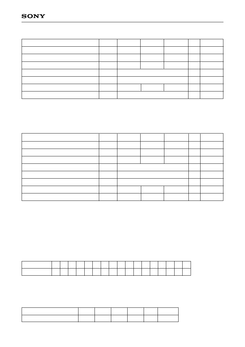
Item
V
DD
V
RD
V
GG
V
SS
V
L
V
DSUB
V
SUB
V
SUB
14.55
14.55
1.75
6.0
–3
15.0
15.0
2.0
3
4
15.45
15.45
2.25
14.0
+3
V
V
V
V
%
V
RD
= V
DD
5
5
Symbol
Min.
Typ.
Max.
Unit
Remarks
Bias Conditions 2 [when used in substrate bias external adjustment mode]
Output circuit supply voltage
Reset drain voltage
Output circuit gate voltage
Output circuit source
Protective transistor bias
Substrate bias circuit supply voltage
Substrate voltage adjustment range
Substrate voltage adjustment precision
3
V
L
setting is the V
VL
voltage of the vertical transfer clock waveform, or the same power supply as the V
L
power supply for the V driver should be used. (When CXD1267AN is used.)
4
Connect to GND or leave open.
5
The setting value of the substrate voltage (V
SUB
) is indicated on the back of the image sensor by a special
code. When adjusting the substrate voltage externally, adjust the substrate voltage to the indicated voltage.
The adjustment precision is ±3%. However, this setting value has not significance when used in substrate
bias internal generation mode.
V
SUB
code — one character indication
Code and optimal setting correspond to each other as follows.
DC Characteristics
Item
Output circuit supply current
I
DD
5.0
10.0
mA
Symbol
Min.
Typ.
Max.
Unit
Remarks
V
SUB
code
Optimal setting 6.0 6.5 7.0 7.5 8.0 8.5 9.0 9.5
10.0 10.5 11.0 11.5 12.0 12.5 13.0 13.5 14.0
E
f
G
h
J
K
L
m
N
P
Q
R
S
T
U
V
W
<Example> "L"
→
V
SUB
= 9.0V
Item
V
DD
V
RD
V
GG
V
SS
V
L
V
DSUB
φ
SUB
14.55
14.55
1.75
Grounded with 390
resistor
14.55
15.0
15.0
2.0
1
15.0
2
15.45
15.45
2.25
15.45
V
V
V
V
V
RD
= V
DD
Symbol
Min.
Typ.
Max.
Unit
Remarks
Bias Conditions 1 [when used in substrate bias internal generation mode]
Output circuit supply voltage
Reset drain voltage
Output circuit gate voltage
Output circuit source
Protective transistor bias
Substrate bias circuit supply voltage
Substrate clock
1
V
L
setting is the V
VL
voltage of the vertical transfer clock waveform, or the same power supply as the V
L
power supply for the V driver should be used. (When CXD1267AN is used.)
2
Do not apply a DC bias to the substrate clock pin, because a DC bias is generated within the CCD.
Grounded with 390
resistor
相关PDF资料 |
PDF描述 |
|---|---|
| ICX252AK | Diagonal 8.933mm (Type 1/1.8) Frame Readout CCD Image Sensor with Square Pixel for Color Cameras |
| ICX252AKF | TRANS ARRAY PNP/NPN MINI-6P |
| ICX252 | Timing Generator for Frame Readout CCD Image Sensor |
| ICX252AQ | Diagonal 8.933mm (Type 1/1.8) Frame Readout CCD Image Sensor with Square Pixel for Color Cameras |
| ICX252AQF | Diagonal 8.933mm (Type 1/1.8) Frame Readout CCD Image Sensor with Square Pixel for Color Cameras |
相关代理商/技术参数 |
参数描述 |
|---|---|
| ICX252 | 制造商:SONY 制造商全称:Sony Corporation 功能描述:Timing Generator and Signal Processor for Frame Readout CCD Image Sensor |
| ICX252AK | 制造商:SONY 制造商全称:Sony Corporation 功能描述:Diagonal 8.933mm (Type 1/1.8) Frame Readout CCD Image Sensor with Square Pixel for Color Cameras |
| ICX252AKF | 制造商:SONY 制造商全称:Sony Corporation 功能描述:Diagonal 8.933mm (Type 1/1.8) Frame Readout CCD Image Sensor with Square Pixel for Color Cameras |
| ICX252AQ | 制造商:SONY 制造商全称:Sony Corporation 功能描述:Diagonal 8.933mm (Type 1/1.8) Frame Readout CCD Image Sensor with Square Pixel for Color Cameras |
| ICX252AQF | 制造商:SONY 制造商全称:Sony Corporation 功能描述:Diagonal 8.933mm (Type 1/1.8) Frame Readout CCD Image Sensor with Square Pixel for Color Cameras |
发布紧急采购,3分钟左右您将得到回复。