- 您现在的位置:买卖IC网 > PDF目录65573 > IDT29FCT52BTSO (INTEGRATED DEVICE TECHNOLOGY INC) FCT SERIES, 8-BIT REGISTERED TRANSCEIVER, TRUE OUTPUT, PDSO24 PDF资料下载
参数资料
| 型号: | IDT29FCT52BTSO |
| 厂商: | INTEGRATED DEVICE TECHNOLOGY INC |
| 元件分类: | 总线收发器 |
| 英文描述: | FCT SERIES, 8-BIT REGISTERED TRANSCEIVER, TRUE OUTPUT, PDSO24 |
| 封装: | SOIC-24 |
| 文件页数: | 3/7页 |
| 文件大小: | 70K |
| 代理商: | IDT29FCT52BTSO |
INDUSTRIALTEMPERATURERANGE
IDT29FCT2052AT/BT/CT
FASTCMOSOCTALREGISTEREDTRANSCEIVER
3
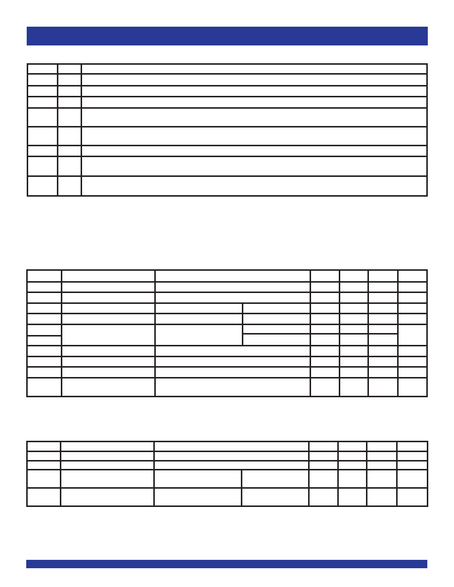
Symbol
Parameter
Test Conditions(1)
Min.
Typ.(2)
Max.
Unit
VIH
Input HIGH Level
Guaranteed Logic HIGH Level
2
—
V
VIL
Input LOW Level
Guaranteed Logic LOW Level
—
0.8
V
IIH
Input HIGH Current(4)
VCC = Max.
VI = 2.7V
—
±1 A
IIL
Input LOW Current(4)
VCC = Max.
VI = 0.5V
—
±1 A
IOZH
High Impedance Output Current
VCC = Max., VI = VCC (Max.)
VI = 2.7V
—
±1 A
IOZL
(3-State Output pins)(4)
VI = 0.5V
—
±1
II
Input HIGH Current(4)
VCC = Max., VI = VCC (Max.)
—
±1 A
VIK
Clamp Diode Voltage
VCC = Min., IIN = –18mA
—
–0.7
–1.2
V
VH
Input Hysteresis
—
200
—
mV
ICC
Quiescent Power Supply Current
VCC = 3V
—
0.01
1
A
VIN = GND or VCC
DC ELECTRICAL CHARACTERISTICS OVER OPERATING RANGE
Following Conditions Apply Unless Otherwise Specified:
Industrial: TA = –40°C to +85°C, VCC = 5.0V ±5%
NOTES:
1. For conditions shown as Min. or Max., use appropriate value specified under Electrical Characteristics for the applicable device type.
2. Typical values are at VCC = 5.0V, +25°C ambient.
3. Not more than one output should be tested at one time. Duration of the test should not exceed one second.
4. The test limit for this parameter is ±5A at TA = –55°C.
Symbol
Parameter
Test Conditions(1)
Min.
Typ.(2)
Max.
Unit
IODL
Output LOW Current
VCC = 5V, VIN = VIH or VIL, VOUT = 1.5V(3)
16
48
—
mA
IODH
Output HIGH Current
VCC = 5V, VIN = VIH or VIL, VOUT = 1.5V(3)
-16
-48
—
mA
VOH
Output HIGH Voltage
VCC = Min
IOH = –15mA
2.4
3.3
—
V
VIN = VIH or VIL
VOL
Output LOW Voltage
VCC = Min
IOL = 12mA
—
0.3
0.5
V
VIN = VIH or VIL
OUTPUT DRIVE CHARACTERISTICS
PIN DESCRIPTION
Name
I/O
Description
A0-7
I/O
Eight bidirectional lines carrying the A Register inputs or B Register outputs
B0-7
I/O
Eight bidirectional lines carrying the B Register inputs or A Register outputs
CPA
I
Clock for the A Register. When
CEA is LOW, data is entered into the A Register on the LOW-to-HIGH transition of the CPA signal.
CEA
I
Clock Enable for the A Register. When
CEA is LOW, data is entered into the A Register on the LOW-to-HIGH transition of the CPA signal. When
CEA is HIGH, the A Register holds its contents, regardless of CPA signal transitions.
OEB
I
Output Enable for the A Register. When
OEBis LOW, the A Register outputs are enabled onto the B0-7 lines. When OEB is HIGH, the B0-7 outputs
areinthehigh-impedancestate.
CPB
I
Clock for the B Register. When
CEB is LOW, data is entered into the B Register on the LOW-to-HIGH transition of the CPB signal.
CEB
I
Clock Enable for the B Register. When
CEB is LOW, data is entered into the B Register on the LOW-to-HIGH transition of the CPB signal. When
CEB is HIGH, the B Register holds its contents, regardless of CPB signal transitions.
OEA
I
Output Enable for the B Register. When
OEAis LOW, the B Register outputs are enabled onto the A0-7 lines. When OEA is HIGH, the A0-7 outputs
areinthehigh-impedancestate.
相关PDF资料 |
PDF描述 |
|---|---|
| IDT29FCT52CTPY8 | FCT SERIES, 8-BIT REGISTERED TRANSCEIVER, TRUE OUTPUT, PDSO24 |
| IDT29FCT52DTSO8 | FCT SERIES, 8-BIT REGISTERED TRANSCEIVER, TRUE OUTPUT, PDSO24 |
| IDT49FCT3805ASOGI | FCT SERIES, LOW SKEW CLOCK DRIVER, 10 TRUE OUTPUT(S), 0 INVERTED OUTPUT(S), PDSO20 |
| IDT49FCT3805AQ8 | FCT SERIES, LOW SKEW CLOCK DRIVER, 10 TRUE OUTPUT(S), 0 INVERTED OUTPUT(S), PDSO20 |
| IDT49FCT3805APYI | FCT SERIES, LOW SKEW CLOCK DRIVER, 10 TRUE OUTPUT(S), 0 INVERTED OUTPUT(S), PDSO20 |
相关代理商/技术参数 |
参数描述 |
|---|---|
| IDT29FCT52C | 制造商:IDT 制造商全称:Integrated Device Technology 功能描述:FAST CMOS OCTAL REGISTERED TRANSCEIVERS |
| IDT29FCT52CD | 制造商:IDT 制造商全称:Integrated Device Technology 功能描述:FAST CMOS OCTAL REGISTERED TRANSCEIVERS |
| IDT29FCT52CDB | 制造商:IDT 制造商全称:Integrated Device Technology 功能描述:FAST CMOS OCTAL REGISTERED TRANSCEIVERS |
| IDT29FCT52CE | 制造商:IDT 制造商全称:Integrated Device Technology 功能描述:FAST CMOS OCTAL REGISTERED TRANSCEIVERS |
| IDT29FCT52CEB | 制造商:IDT 制造商全称:Integrated Device Technology 功能描述:FAST CMOS OCTAL REGISTERED TRANSCEIVERS |
发布紧急采购,3分钟左右您将得到回复。