- 您现在的位置:买卖IC网 > PDF目录377236 > IDT54FCT841BTPB (Integrated Device Technology, Inc.) FAST CMOS BUS INTERFACE LATCHES PDF资料下载
参数资料
| 型号: | IDT54FCT841BTPB |
| 厂商: | Integrated Device Technology, Inc. |
| 英文描述: | FAST CMOS BUS INTERFACE LATCHES |
| 中文描述: | 快速CMOS总线接口锁存 |
| 文件页数: | 2/7页 |
| 文件大小: | 138K |
| 代理商: | IDT54FCT841BTPB |
6.22
2
MILITARY AND COMMERCIAL TEMPERATURE RANGES
IDT54/74FCT841AT/BT/CT/DT
FAST CMOS BUS INTERFACE LATCHES
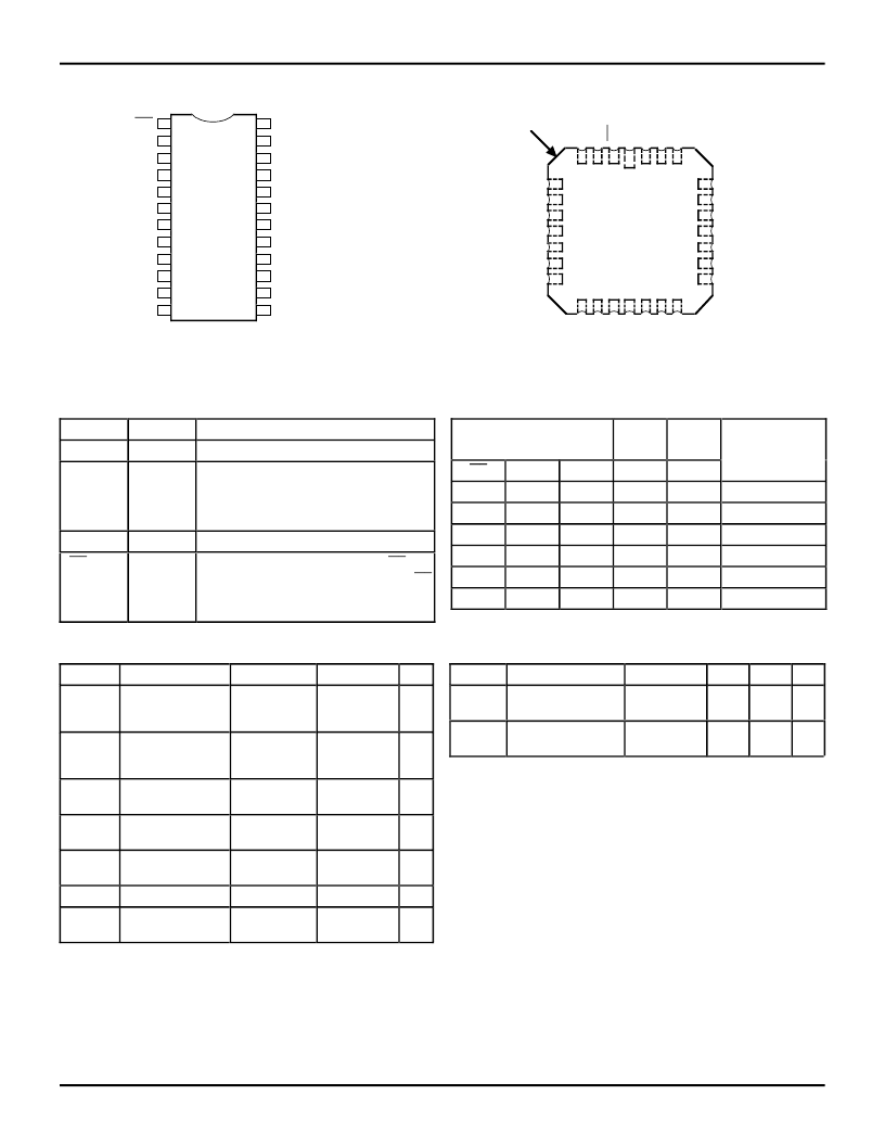
PIN CONFIGURATIONS
2571 drw 02
2571 drw 03
INDEX
D
2
D
3
D
4
NC
D
5
D
6
D
7
Y
2
Y
3
Y
4
NC
Y
5
Y
6
Y
7
O
D
1
N
V
C
Y
0
D
8
G
L
Y
9
Y
8
LCC
TOP VIEW
3 2
20
19
1
4
5
6
7
8
9
10
11
18
17
16
15
14
1213
L28-1
D
0
Y
1
21
22
23
24
25
26
27
28
D
9
N
OE
D
0
D
1
D
2
D
3
D
4
D
5
D
6
D
7
D
8
D
9
GND
Y
0
Y
1
Y
2
Y
3
Y
4
Y
5
Y
6
Y
7
Y
8
Y
9
LE
V
CC
1
2
3
4
5
6
7
8
9
10
11
12
13
14
15
16
17
18
19
20
P24-1
D24-1
SO24-2
SO24-7
SO24-8
&
E24-1
21
22
23
24
DIP/SOIC/SSOP/QSOP/CERPACK
TOP VIEW
PIN DESCRIPTION
FUNCTION TABLE
(1)
2571 tbl 01
NOTE:
1. H = HIGH, L = LOW, X = Don’t Care, NC = No Change, Z = High Impedance
CAPACITANCE
(T
A
= +25
°
C, f = 1.0MHz)
Symbol
Parameter
(1)
Conditions
C
IN
Input
Capacitance
C
OUT
Output
Capacitance
2571 tbl 02
ABSOLUTE MAXIMUM RATINGS
(1)
Symbol
Rating
V
TERM(2)
Terminal Voltage
with Respect to
GND
V
TERM(3)
Terminal Voltage
with Respect to
GND
T
A
Operating
Temperature
T
BIAS
Temperature
Under Bias
T
STG
Storage
Temperature
P
T
Power Dissipation
Commercial
–0.5 to +7.0
Military
–0.5 to +7.0
Unit
V
–0.5 to
V
CC
+0.5
–0.5 to
V
CC
+0.5
V
0 to +70
–55 to +125
°
C
–55 to +125
–65 to +135
°
C
–55 to +125
–65 to +150
°
C
0.5
0.5
W
I
OUT
DC Output
Current
–60 to +120 –60 to +120 mA
2571 lnk 03
NOTE:
1. This parameter is measured at characterization but not tested.
2571 lnk 04
Typ.
6
Max. Unit
10
V
IN
= 0V
pF
V
OUT
= 0V
8
12
pF
NOTES:
1. Stresses greater than those listed under ABSOLUTE MAXIMUM RAT-
INGS may cause permanent damage to the device. This is a stress rating
only and functional operation of the device at these or any other conditions
above those indicated in the operational sections of this specification is
not
implied. Exposure to absolute maximum rating conditions for
extended periods may affect reliability. No terminal voltage may exceed
V
CC
by +0.5V unless otherwise noted.
2. Input and V
CC
terminals only.
3. Outputs and I/O terminals only.
Name
D
I
LE
I/O
I
I
Description
The latch data inputs.
The latch enable input. The latches are
transparent when LE is HIGH. Input data
is latched on the HIGH-to-LOW
transition.
The 3-state latch outputs.
The output enable control. When
OE
is
LOW, the outputs are enabled. When
OE
is HIGH, the outputs VI
are in high-
impedance (off) state.
Y
I
OE
O
I
Inputs
LE
H
Internal Output
Q
I
L
OE
D
I
L
Y
I
Z
Function
High Z
H
H
H
L
H
L
H
H
X
L
H
NC
L
Z
Z
L
High Z
Latched (High Z)
Transparent
L
L
H
L
H
X
H
NC
H
NC
Transparent
Latched
相关PDF资料 |
PDF描述 |
|---|---|
| IDT74FCT841CTQB | FAST CMOS BUS INTERFACE LATCHES |
| IDT74FCT841CTSO | FAST CMOS BUS INTERFACE LATCHES |
| IDT74FCT841CTSOB | FAST CMOS BUS INTERFACE LATCHES |
| IDT74FCT841DT | FAST CMOS BUS INTERFACE LATCHES |
| IDT74FCT841DTD | FAST CMOS BUS INTERFACE LATCHES |
相关代理商/技术参数 |
参数描述 |
|---|---|
| IDT54FCT845ADB | 制造商:Integrated Device Technology Inc 功能描述: |
| IDT54FCT861ADB | 制造商:Integrated Device Technology Inc 功能描述: |
| IDT54FCT861BDB | 制造商:Integrated Device Technology Inc 功能描述: |
| IDT557GI-05ALF | 制造商: 功能描述: 制造商:undefined 功能描述: |
| IDT557GI-06LF | 制造商: 功能描述: 制造商:undefined 功能描述: |
发布紧急采购,3分钟左右您将得到回复。