- 您现在的位置:买卖IC网 > PDF目录67712 > IDT5T93GL161PFGI (INTEGRATED DEVICE TECHNOLOGY INC) 5T SERIES, LOW SKEW CLOCK DRIVER, 16 TRUE OUTPUT(S), 0 INVERTED OUTPUT(S), PQFP64 PDF资料下载
参数资料
| 型号: | IDT5T93GL161PFGI |
| 厂商: | INTEGRATED DEVICE TECHNOLOGY INC |
| 元件分类: | 时钟及定时 |
| 英文描述: | 5T SERIES, LOW SKEW CLOCK DRIVER, 16 TRUE OUTPUT(S), 0 INVERTED OUTPUT(S), PQFP64 |
| 封装: | GREEN, TQFP-64 |
| 文件页数: | 2/14页 |
| 文件大小: | 153K |
| 代理商: | IDT5T93GL161PFGI |
INDUSTRIALTEMPERATURERANGE
10
IDT5T93GL161
2.5VLVDS1:16GLITCHLESSCLOCKBUFFERTERABUFFERII
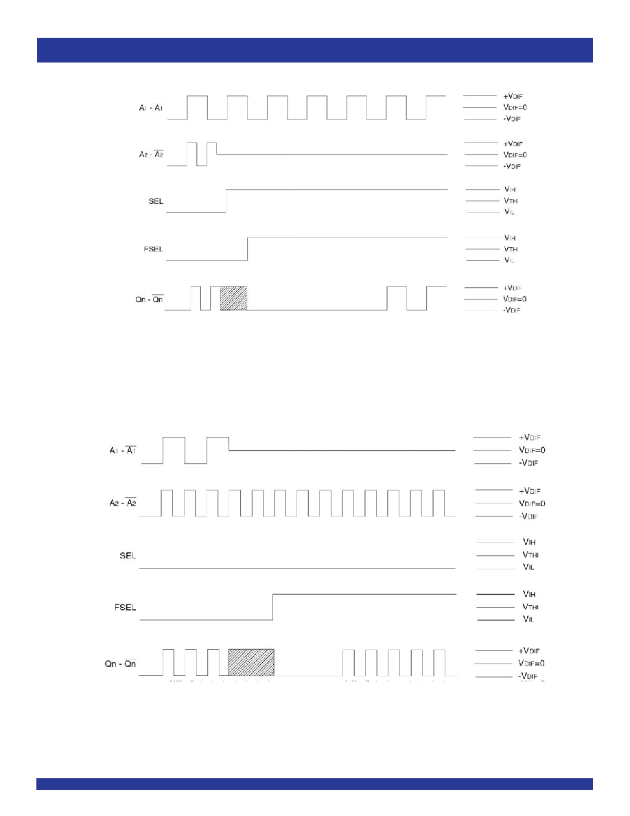
FSEL Operation for When Opposite Clock Dies
NOTES:
1. When the differential on the selected clock goes below the minimum DC differential, the outputs clock goes to an unknown state. When this happens, the SEL pin should be toggled
and FSEL asserted in order to force selection of the new input clock. The output clock will start up after a number of cycles of the newly-selected input clock.
2. The FSEL pin should stay asserted until the problem with the dead clock can be fixed in the system.
3. It is recommended that the FSEL be tied HIGH for systems that use only one input. If this is not possible, the user must guarantee that the unused input have a differential greater
than or equal to the minimum DC differential specified in the datasheet.
FSEL Operation for When Current Clock Dies
NOTES:
1. When the differential on the non-selected clock goes below the minimum DC differential, the outputs clock goes to an unknown state. When this happens, the FSEL pin should
be asserted in order to force selection of the new input clock. The output clock will start up after a number of cycles of the newly-selected input clock.
2. The FSEL pin should stay asserted until the problem with the dead clock can be fixed in the system.
3. It is recommended that the FSEL be tied HIGH for systems that use only one input. If this is not possible, the user must guarantee that the unused input have a differential greater
than or equal to the minimum DC differential specified in the datasheet.
相关PDF资料 |
PDF描述 |
|---|---|
| IDT5T93GL16NLGI | 5T SERIES, LOW SKEW CLOCK DRIVER, 16 TRUE OUTPUT(S), 0 INVERTED OUTPUT(S), PQCC52 |
| IDT5T940-30NLGI8 | 5T SERIES, PLL BASED CLOCK DRIVER, 2 TRUE OUTPUT(S), 0 INVERTED OUTPUT(S), PQCC28 |
| IDT5T940-10NLGI | 5T SERIES, PLL BASED CLOCK DRIVER, 2 TRUE OUTPUT(S), 0 INVERTED OUTPUT(S), PQCC28 |
| IDT5T9820NLGI8 | 5T SERIES, PLL BASED CLOCK DRIVER, 10 TRUE OUTPUT(S), 0 INVERTED OUTPUT(S), QCC68 |
| IDT5T9820NLGI | 5T SERIES, PLL BASED CLOCK DRIVER, 10 TRUE OUTPUT(S), 0 INVERTED OUTPUT(S), QCC68 |
相关代理商/技术参数 |
参数描述 |
|---|---|
| IDT5T93GL161PFGI8 | 功能描述:IC CLOCK BUFFER MUX 2:16 64-TQFP RoHS:是 类别:集成电路 (IC) >> 时钟/计时 - 时钟缓冲器,驱动器 系列:TERABUFFER™ II 标准包装:74 系列:- 类型:扇出缓冲器(分配) 电路数:1 比率 - 输入:输出:1:10 差分 - 输入:输出:是/是 输入:HCSL, LVCMOS, LVDS, LVPECL, LVTTL 输出:HCSL,LVDS 频率 - 最大:400MHz 电源电压:3 V ~ 3.6 V 工作温度:-40°C ~ 85°C 安装类型:表面贴装 封装/外壳:32-VFQFN 裸露焊盘 供应商设备封装:32-QFN(5x5) 包装:管件 |
| IDT5T93GL16NLGI | 功能描述:IC CLK BUFFER MUX 2:16 52-VFQFPN RoHS:是 类别:集成电路 (IC) >> 时钟/计时 - 时钟缓冲器,驱动器 系列:TERABUFFER™ II 标准包装:74 系列:- 类型:扇出缓冲器(分配) 电路数:1 比率 - 输入:输出:1:10 差分 - 输入:输出:是/是 输入:HCSL, LVCMOS, LVDS, LVPECL, LVTTL 输出:HCSL,LVDS 频率 - 最大:400MHz 电源电压:3 V ~ 3.6 V 工作温度:-40°C ~ 85°C 安装类型:表面贴装 封装/外壳:32-VFQFN 裸露焊盘 供应商设备封装:32-QFN(5x5) 包装:管件 |
| IDT5T93GL16NLGI8 | 功能描述:IC CLK BUFFER MUX 2:16 52-VFQFPN RoHS:是 类别:集成电路 (IC) >> 时钟/计时 - 时钟缓冲器,驱动器 系列:TERABUFFER™ II 标准包装:74 系列:- 类型:扇出缓冲器(分配) 电路数:1 比率 - 输入:输出:1:10 差分 - 输入:输出:是/是 输入:HCSL, LVCMOS, LVDS, LVPECL, LVTTL 输出:HCSL,LVDS 频率 - 最大:400MHz 电源电压:3 V ~ 3.6 V 工作温度:-40°C ~ 85°C 安装类型:表面贴装 封装/外壳:32-VFQFN 裸露焊盘 供应商设备封装:32-QFN(5x5) 包装:管件 |
| IDT5T940-10NLGI | 功能描述:IC CLK GENERATOR PREC 28-VFQFPN RoHS:是 类别:集成电路 (IC) >> 时钟/计时 - 专用 系列:- 标准包装:1,500 系列:- 类型:时钟缓冲器/驱动器 PLL:是 主要目的:- 输入:- 输出:- 电路数:- 比率 - 输入:输出:- 差分 - 输入:输出:- 频率 - 最大:- 电源电压:3.3V 工作温度:0°C ~ 70°C 安装类型:表面贴装 封装/外壳:28-SSOP(0.209",5.30mm 宽) 供应商设备封装:28-SSOP 包装:带卷 (TR) 其它名称:93786AFT |
| IDT5T940-10NLGI8 | 功能描述:IC CLK GENERATOR PREC 28-VFQFPN RoHS:是 类别:集成电路 (IC) >> 时钟/计时 - 专用 系列:- 标准包装:1,500 系列:- 类型:时钟缓冲器/驱动器 PLL:是 主要目的:- 输入:- 输出:- 电路数:- 比率 - 输入:输出:- 差分 - 输入:输出:- 频率 - 最大:- 电源电压:3.3V 工作温度:0°C ~ 70°C 安装类型:表面贴装 封装/外壳:28-SSOP(0.209",5.30mm 宽) 供应商设备封装:28-SSOP 包装:带卷 (TR) 其它名称:93786AFT |
发布紧急采购,3分钟左右您将得到回复。