- 您现在的位置:买卖IC网 > PDF目录4033 > IDT70V07S55J8 (IDT, Integrated Device Technology Inc)IC SRAM 256KBIT 55NS 68PLCC PDF资料下载
参数资料
| 型号: | IDT70V07S55J8 |
| 厂商: | IDT, Integrated Device Technology Inc |
| 文件页数: | 9/19页 |
| 文件大小: | 0K |
| 描述: | IC SRAM 256KBIT 55NS 68PLCC |
| 标准包装: | 250 |
| 格式 - 存储器: | RAM |
| 存储器类型: | SRAM - 双端口,异步 |
| 存储容量: | 256K (32K x 8) |
| 速度: | 55ns |
| 接口: | 并联 |
| 电源电压: | 3 V ~ 3.6 V |
| 工作温度: | 0°C ~ 70°C |
| 封装/外壳: | 68-LCC(J 形引线) |
| 供应商设备封装: | 68-PLCC(24x24) |
| 包装: | 带卷 (TR) |
| 其它名称: | 70V07S55J8 |
�� �
�
�IDT70V07S/L�
�High-Speed� 32K� x� 8� Dual-Port� Static� RAM�
�Industrial� and� Commercial� Temperature� Ranges�
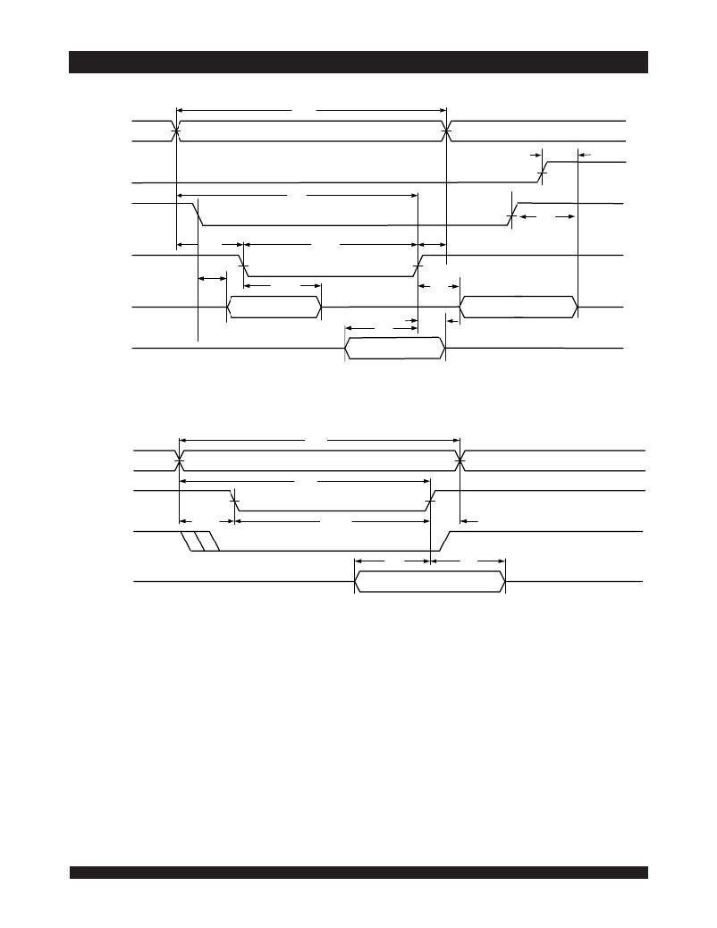
�Timing� Waveform� of� Write� Cycle� No.� 1,� R/� W� Controlled� Timing� (1,5,8)�
�t� WC�
�ADDRESS�
�t� HZ� (7)�
�OE�
�t� AW�
�CE� or� SEM�
�(9)�
�t� HZ� (7)�
�R/� W�
�DATA� OUT�
�t� AS� (6)�
�t� LZ�
�t� WZ� (7)�
�(4)�
�t� WP� (2)�
�t� OW�
�t� WR� (3)�
�(4)�
�DATA� IN�
�t� DW�
�t� DH�
�,�
�CE� or� SEM�
�2943� drw� 09�
�Timing� Waveform� of� Write� Cycle� No.� 2,� CE� Controlled� Timing� (1,5)�
�t� WC�
�ADDRESS�
�t� AW�
�(9)�
�t� WR�
�R/� W�
�t� AS� (6)�
�t� EW� (2)�
�t� DW�
�(3)�
�t� DH�
�DATA� IN�
�2943� drw� 10�
�NOTES:�
�1.� R/� W� or� CE� must� be� HIGH� during� all� address� transitions.�
�2.� A� write� occurs� during� the� overlap� (t� EW� or� t� WP� )� of� a� LOW� CE� and� a� LOW� R/� W� for� memory� array� writing� cycle.�
�3.� t� WR� is� measured� from� the� earlier� of� CE� or� R/� W� (or� SEM� or� R/� W� )� going� HIGH� to� the� end� of� write� cycle.�
�4.� During� this� period,� the� I/O� pins� are� in� the� output� state� and� input� signals� must� not� be� applied.�
�5.� If� the� CE� or� SEM� LOW� transition� occurs� simultaneously� with� or� after� the� R/� W� LOW� transition,� the� outputs� remain� in� the� High-impedance� state.�
�6.� Timing� depends� on� which� enable� signal� is� asserted� last,� CE� or� R/� W� .�
�7.� This� parameter� is� guaranteed� by� device� characterization,� but� is� not� production� tested.� Transition� is� measured� 0mV� from� steady� state� with� the� Output� Test� Load�
�(Figure� 2).�
�8.� If� OE� is� LOW� during� R/� W� controlled� write� cycle,� the� write� pulse� width� must� be� the� larger� of� t� WP� or� (t� WZ� +� t� DW� )� to� allow� the� I/O� drivers� to� turn� off� and� data� to� be� placed� on� the�
�bus� for� the� required� t� DW� .� If� OE� is� HIGH� during� an� R/W� controlled� write� cycle,� this� requirement� does� not� apply� and� the� write� pulse� can� be� as� short� as� the� specified� t� WP� .�
�9.� To� access� SRAM,� CE� =� V� IL� and� SEM� =� V� IH� .� To� access� semaphore,� CE� =� V� IH� and� SEM� =� V� IL� .� t� EW� must� be� met� for� either� condition.�
�9�
�相关PDF资料 |
PDF描述 |
|---|---|
| MC7448VS1267ND | IC MPU RISC 1267MHZ 360-FCCLGA |
| KMC7448VU1700LD | IC MPU 128BIT 1700MHZ 360-FCCBGA |
| KMC7448HX1267ND | IC MPU 128BIT 1267MHZ 360-FCCBGA |
| IDT7007S55J8 | IC SRAM 256KBIT 55NS 68PLCC |
| P4080NSN1NNB | IC MPU 1333MHZ |
相关代理商/技术参数 |
参数描述 |
|---|---|
| IDT70V07S55PF | 功能描述:IC SRAM 256KBIT 55NS 80TQFP RoHS:否 类别:集成电路 (IC) >> 存储器 系列:- 标准包装:1,000 系列:- 格式 - 存储器:RAM 存储器类型:SRAM - 双端口,同步 存储容量:1.125M(32K x 36) 速度:5ns 接口:并联 电源电压:3.15 V ~ 3.45 V 工作温度:-40°C ~ 85°C 封装/外壳:256-LBGA 供应商设备封装:256-CABGA(17x17) 包装:带卷 (TR) 其它名称:70V3579S5BCI8 |
| IDT70V07S55PF8 | 功能描述:IC SRAM 256KBIT 55NS 80TQFP RoHS:否 类别:集成电路 (IC) >> 存储器 系列:- 标准包装:45 系列:- 格式 - 存储器:RAM 存储器类型:SRAM - 双端口,异步 存储容量:128K(8K x 16) 速度:15ns 接口:并联 电源电压:3 V ~ 3.6 V 工作温度:0°C ~ 70°C 封装/外壳:100-LQFP 供应商设备封装:100-TQFP(14x14) 包装:托盘 其它名称:70V25S15PF |
| IDT70V08L15PF | 功能描述:IC SRAM 512KBIT 15NS 100TQFP RoHS:否 类别:集成电路 (IC) >> 存储器 系列:- 标准包装:1,000 系列:- 格式 - 存储器:RAM 存储器类型:SRAM - 双端口,同步 存储容量:1.125M(32K x 36) 速度:5ns 接口:并联 电源电压:3.15 V ~ 3.45 V 工作温度:-40°C ~ 85°C 封装/外壳:256-LBGA 供应商设备封装:256-CABGA(17x17) 包装:带卷 (TR) 其它名称:70V3579S5BCI8 |
| IDT70V08L15PF8 | 功能描述:IC SRAM 512KBIT 15NS 100TQFP RoHS:否 类别:集成电路 (IC) >> 存储器 系列:- 标准包装:1,000 系列:- 格式 - 存储器:RAM 存储器类型:SRAM - 双端口,同步 存储容量:1.125M(32K x 36) 速度:5ns 接口:并联 电源电压:3.15 V ~ 3.45 V 工作温度:-40°C ~ 85°C 封装/外壳:256-LBGA 供应商设备封装:256-CABGA(17x17) 包装:带卷 (TR) 其它名称:70V3579S5BCI8 |
| IDT70V08L15PFG | 功能描述:IC SRAM 512KBIT 15NS 100TQFP RoHS:是 类别:集成电路 (IC) >> 存储器 系列:- 标准包装:1,000 系列:- 格式 - 存储器:RAM 存储器类型:SRAM - 双端口,同步 存储容量:1.125M(32K x 36) 速度:5ns 接口:并联 电源电压:3.15 V ~ 3.45 V 工作温度:-40°C ~ 85°C 封装/外壳:256-LBGA 供应商设备封装:256-CABGA(17x17) 包装:带卷 (TR) 其它名称:70V3579S5BCI8 |
发布紧急采购,3分钟左右您将得到回复。