- 您现在的位置:买卖IC网 > PDF目录377311 > IDT7143LA25JB (INTEGRATED DEVICE TECHNOLOGY INC) HIGH-SPEED 2K x 16 CMOS DUAL-PORT STATIC RAMS PDF资料下载
参数资料
| 型号: | IDT7143LA25JB |
| 厂商: | INTEGRATED DEVICE TECHNOLOGY INC |
| 元件分类: | DRAM |
| 英文描述: | HIGH-SPEED 2K x 16 CMOS DUAL-PORT STATIC RAMS |
| 中文描述: | 2K X 16 DUAL-PORT SRAM, 25 ns, PQCC68 |
| 封装: | PLASTIC, LCC-68 |
| 文件页数: | 9/16页 |
| 文件大小: | 140K |
| 代理商: | IDT7143LA25JB |
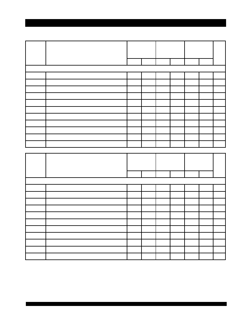
6.42
IDT7133SA/LA, IDT7143SA/LA
High-Speed 2K x 16 Dual-Port RAM Military, Industrial and Commercial Temperature Ranges
%*.5*
.$-123
(!
NOTES:
1. Transition is measured 0mV fromLow or High-impedance voltage fromthe Output Test Load (Figure 2).
2.
This parameter is guaranteed by device characterization but not production tested.
3.
For MASTER/SLAVE combination, t
WC
= t
BAA
+ t
WR
+ t
WP
, since R/
W
= V
IL
must occur after t
BAA.
4.
The specification for t
DH
must be met by the device supplying write data to the RAMunder all operation conditions. Although t
DH
and t
OW
values will very over voltage and
temperature, the actual t
DH
will always be smaller than the actual t
OW
.
5.
'X' in part number indicates power rating (SA or LA).
Symbol
Parameter
7133X20
7143X20
Com'l Only
7133X25
7143X25
Com'l, Ind
& Mlitary
7133X35
7143X35
Com'l, Ind
& Mlitary
Unit
Mn.
Max.
Mn.
Max.
Mn.
Max.
WRITE CYCLE
t
WC
Write Cycle Time
(3)
20
____
25
____
35
____
ns
t
EW
Chip Enable to End-of-Write
15
____
20
____
25
____
ns
t
AW
Address Valid to End-of-Write
15
____
20
____
25
____
ns
t
AS
Address Set-up Time
0
____
0
____
0
____
ns
t
WP
Write Pulse Width
15
____
20
____
25
____
ns
t
WR
Write Recovery Time
0
____
0
____
0
____
ns
t
DW
Data Valid to End-of-Write
15
____
15
____
20
____
ns
t
HZ
Output High-Z Time
(1,2)
____
12
____
15
____
20
ns
t
DH
Data Hold Time
(4)
0
____
0
____
0
____
ns
t
WZ
Write Enable to Output in High-Z
(1,2)
____
12
____
15
____
20
ns
t
OW
Output Active fromEnd-of-Write
(1,2,4)
0
____
0
____
0
____
ns
2746 tbl 11a
Symbol
Parameter
7133X45
7143X45
Com'l &
Mlitary
7133X55
7143X55
Com'l, Ind
& Mlitary
7133X70/90
7143X70/90
Com'l &
Mlitary
Unit
Mn.
Max.
Mn.
Max.
Mn.
Max.
WRITE CYCLE
t
WC
Write Cycle Time
(3)
45
____
55
____
70/90
____
ns
t
EW
Chip Enable to End-of-Write
30
____
40
____
50/50
____
ns
t
AW
Address Valid to End-of-Write
30
____
40
____
50/50
____
ns
t
AS
Address Set-up Time
0
____
0
____
0/0
____
ns
t
WP
Write Pulse Width
30
____
40
____
50/50
____
ns
t
WR
Write Recovery Time
0
____
0
____
0/0
____
ns
t
DW
Data Valid to End-of-Write
20
____
25
____
30/30
____
ns
t
HZ
Output High-Z Time
(1,2)
____
20
____
20
____
25/25
ns
t
DH
Data Hold Time
(4)
5
____
5
____
5/5
____
ns
t
WZ
Write Enable to Output in High-Z
(1,2)
____
20
____
20
____
25/25
ns
t
OW
Output Active fromEnd-of-Write
(1,2,4)
5
____
5
____
5/5
____
ns
2746 tbl 11b
相关PDF资料 |
PDF描述 |
|---|---|
| IDT7133LA25JI | HIGH-SPEED 2K x 16 CMOS DUAL-PORT STATIC RAMS |
| IDT7143LA25JI | HIGH-SPEED 2K x 16 CMOS DUAL-PORT STATIC RAMS |
| IDT7133SA25JI | HIGH-SPEED 2K x 16 CMOS DUAL-PORT STATIC RAMS |
| IDT7143SA25JI | HIGH-SPEED 2K x 16 CMOS DUAL-PORT STATIC RAMS |
| IDT7133LA45PF | SILICONE COATED MIL GRADE WIREWOUND RESISTOR AXIAL LEAD , 100 OHM, 0.01%, ROHS |
相关代理商/技术参数 |
参数描述 |
|---|---|
| IDT7143LA25JGI | 制造商:Integrated Device Technology Inc 功能描述: |
| IDT7143LA25JI | 功能描述:IC SRAM 32KBIT 25NS 68PLCC RoHS:否 类别:集成电路 (IC) >> 存储器 系列:- 标准包装:45 系列:- 格式 - 存储器:RAM 存储器类型:SRAM - 双端口,异步 存储容量:128K(8K x 16) 速度:15ns 接口:并联 电源电压:3 V ~ 3.6 V 工作温度:0°C ~ 70°C 封装/外壳:100-LQFP 供应商设备封装:100-TQFP(14x14) 包装:托盘 其它名称:70V25S15PF |
| IDT7143LA25JI8 | 功能描述:IC SRAM 32KBIT 25NS 68PLCC RoHS:否 类别:集成电路 (IC) >> 存储器 系列:- 标准包装:72 系列:- 格式 - 存储器:RAM 存储器类型:SRAM - 同步 存储容量:9M(256K x 36) 速度:75ns 接口:并联 电源电压:3.135 V ~ 3.465 V 工作温度:-40°C ~ 85°C 封装/外壳:100-LQFP 供应商设备封装:100-TQFP(14x14) 包装:托盘 其它名称:71V67703S75PFGI |
| IDT7143LA25PF | 功能描述:IC SRAM 32KBIT 25NS 100TQFP RoHS:否 类别:集成电路 (IC) >> 存储器 系列:- 标准包装:45 系列:- 格式 - 存储器:RAM 存储器类型:SRAM - 双端口,异步 存储容量:128K(8K x 16) 速度:15ns 接口:并联 电源电压:3 V ~ 3.6 V 工作温度:0°C ~ 70°C 封装/外壳:100-LQFP 供应商设备封装:100-TQFP(14x14) 包装:托盘 其它名称:70V25S15PF |
| IDT7143LA25PF8 | 功能描述:IC SRAM 32KBIT 25NS 100TQFP RoHS:否 类别:集成电路 (IC) >> 存储器 系列:- 标准包装:72 系列:- 格式 - 存储器:RAM 存储器类型:SRAM - 同步 存储容量:9M(256K x 36) 速度:75ns 接口:并联 电源电压:3.135 V ~ 3.465 V 工作温度:-40°C ~ 85°C 封装/外壳:100-LQFP 供应商设备封装:100-TQFP(14x14) 包装:托盘 其它名称:71V67703S75PFGI |
发布紧急采购,3分钟左右您将得到回复。