- 您现在的位置:买卖IC网 > PDF目录10092 > IDT72221L10J8 (IDT, Integrated Device Technology Inc)IC FIFO SYNC 1KX9 10NS 32PLCC PDF资料下载
参数资料
| 型号: | IDT72221L10J8 |
| 厂商: | IDT, Integrated Device Technology Inc |
| 文件页数: | 10/14页 |
| 文件大小: | 0K |
| 描述: | IC FIFO SYNC 1KX9 10NS 32PLCC |
| 标准包装: | 750 |
| 系列: | 7200 |
| 功能: | 同步 |
| 存储容量: | 9K(1K x 9) |
| 数据速率: | 100MHz |
| 访问时间: | 10ns |
| 电源电压: | 4.5 V ~ 5.5 V |
| 工作温度: | 0°C ~ 70°C |
| 安装类型: | 表面贴装 |
| 封装/外壳: | 32-LCC(J 形引线) |
| 供应商设备封装: | 32-PLCC(13.97x11.43) |
| 包装: | 带卷 (TR) |
| 其它名称: | 72221L10J8 |
5
COMMERCIALANDINDUSTRIAL
TEMPERATURERANGES
IDT72421/72201/72211/72221/72231/72241/72251 CMOS SyncFIFO
64 x 9, 256 x 9, 512 x 9, 1,024 x 9, 2,048 x 9, 4,096 x 9 and 8,192 x 9
OUTPUT ENABLE (OE)
When Output Enable (OE) is enabled (LOW), the parallel output buffers
receive data from the output register. When Output Enable (OE) is disabled
(HIGH), the Q output data bus is in a high-impedance state.
WRITE ENABLE 2/LOAD (WEN2/LD)
This is a dual-purpose pin. The FIFO is configured at Reset to have
programmableflagsortohavetwowriteenables,whichallowsdepthexpansion.
IfWriteEnable2/Load(WEN2/LD)issetHIGHatReset(RS =LOW),thispin
operates as a second write enable pin.
If the FIFO is configured to have two write enables, when Write Enable
(WEN1) is LOW and Write Enable 2/Load (WEN2/LD) is HIGH, data can be
loaded into the input register and RAM array on the LOW-to-HIGH transition
ofeveryWriteClock(WCLK). DataisstoredintheRAMarraysequentiallyand
independently of any ongoing read operation.
In this configuration, when Write Enable (WEN1) is HIGH and/or Write
Enable2/Load(WEN2/LD)isLOW,theinputregisterholdsthepreviousdata
and no new data is allowed to be loaded into the register.
Topreventdataoverflow,theFullFlag(FF)willgoLOW,inhibitingfurther
writeoperations. Uponthecompletionofavalidreadcycle,theFullFlag(FF)
willgoHIGHaftertWFF,allowingavalidwritetobegin. WriteEnable1(WEN1)
and Write Enable 2/Load (WEN2/LD) are ignored when the FIFO is full.
TheFIFOisconfiguredtohaveprogrammableflagswhentheWriteEnable
2/Load (WEN2/LD) is set LOW at Reset (RS=LOW). The IDT72421/72201/
72211/72221/72231/72241/72251devicescontainfour8-bitoffsetregisters
whichcanbeloadedwithdataontheinputs,orreadontheoutputs. SeeFigure
3 for details of the size of the registers and the default values.
IftheFIFOisconfiguredtohaveprogrammableflagswhentheWriteEnable
1(WEN1)andWriteEnable2/Load(WEN2/LD)aresetLOW,dataontheinputs
DiswrittenintotheEmpty(LeastSignificantBit)OffsetregisteronthefirstLOW-
to-HIGHtransitionoftheWriteClock(WCLK). DataiswrittenintotheEmpty(Most
SignificantBit)OffsetregisteronthesecondLOW-to-HIGHtransitionoftheWrite
Clock (WCLK), into the Full (Least Significant Bit) Offset register on the third
transition, and into the Full (Most Significant Bit) Offset register on the fourth
transition. ThefifthtransitionoftheWriteClock(WCLK)againwritestotheEmpty
(LeastSignificantBit)Offsetregister.
However,writingalloffsetregistersdoesnothavetooccuratonetime. One
ortwooffsetregisterscanbewrittenandthenbybringingtheWriteEnable2/
Load (WEN2/LD) pin HIGH, the FIFO is returned to normal read/write
operation. WhentheWriteEnable2/Load(WEN2/LD)pinissetLOW,theWrite
Enable 1 (WEN1) is LOW, the next offset register in sequence is written.
SIGNAL DESCRIPTIONS
INPUTS:
DATA IN (D0 - D8)
Data inputs for 9-bit wide data.
CONTROLS:
RESET (RS)
Reset is accomplished whenever the Reset (RS) input is taken to a LOW
state. During reset, both internal read and write pointers are set to the first
location. A reset is required after power-up before a write operation can take
place. TheFullFlag(FF)andProgrammableAlmost-Fullflag(PAF)willbereset
to HIGH after tRSF. The Empty Flag (EF) and Programmable Almost-Empty
flag(PAE)willberesettoLOWaftertRSF. Duringreset,theoutputregisteris
initializedtoallzerosandtheoffsetregistersareinitializedtotheirdefaultvalues.
WRITE CLOCK (WCLK)
AwritecycleisinitiatedontheLOW-to-HIGHtransitionoftheWriteClock
(WCLK). DatasetupandholdtimesmustbemetinrespecttotheLOW-to-HIGH
transition of WCLK. The Full Flag (FF) and Programmable Almost-Full flag
(PAF)aresynchronizedwithrespecttotheLOW-to-HIGHtransitionofWCLK.
The Write and Read Clocks can be asynchronous or coincident.
WRITE ENABLE 1 (WEN1)
If the FIFO is configured for programmable flags, Write Enable 1 (WEN1)
istheonlyenablecontrolpin. Inthisconfiguration,whenWriteEnable1(WEN1)
isLOW,datacanbeloadedintotheinputregisterandRAMarrayontheLOW-
to-HIGHtransitionofeveryWriteClock(WCLK). DataisstoredintheRAMarray
sequentially and independently of any ongoing read operation.
Inthisconfiguration,whenWriteEnable1(WEN1)isHIGH,theinputregister
holdsthepreviousdataandnonewdataisallowedtobeloadedintotheregister.
IftheFIFOisconfiguredtohavetwowriteenables,whichallowsfordepth
expansion,therearetwoenablecontrolpins. SeeWriteEnable2paragraph
belowforoperationinthisconfiguration.
Topreventdataoverflow,theFullFlag(FF)willgoLOW,inhibitingfurther
writeoperations. Uponthecompletionofavalidreadcycle,theFullFlag(FF)
willgoHIGHaftertWFF,allowingavalidwritetobegin. WriteEnable1(WEN1)
is ignored when the FIFO is full.
READ CLOCK (RCLK)
DatacanbereadontheoutputsontheLOW-to-HIGHtransitionoftheRead
Clock (RCLK). The Empty Flag (EF) and Programmable Almost-Empty flag
(PAE)aresynchronizedwithrespecttotheLOW-to-HIGHtransitionofRCLK.
The Write and Read Clocks can be asynchronous or coincident.
READ ENABLES (REN1, REN2)
When both Read Enables (REN1, REN2) are LOW, data is read from the
RAM array to the output register on the LOW-to-HIGH transition of the Read
Clock (RCLK).
WheneitherReadEnable(REN1,REN2)isHIGH,theoutputregisterholds
the previous data and no new data is allowed to be loaded into the register.
When all the data has been read from the FIFO, the Empty Flag (EF) will
go LOW, inhibiting further read operations. Once a valid write operation has
been accomplished, the Empty Flag (EF) will go HIGH after tREF and a valid
readcanbegin. TheReadEnables(REN1,REN2)areignoredwhentheFIFO
isempty.
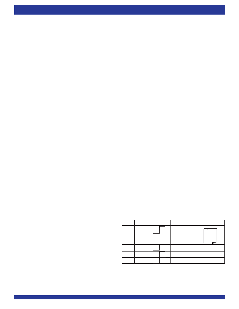
LD
WEN1
WCLK
Selection
0
EmptyOffset(LSB)
Empty Offset (MSB)
Full Offset (LSB)
Full Offset (MSB)
0
1
No Operation
1
0
Write Into FIFO
1
No Operation
NOTE:
1. For the purposes of this table, WEN2 = VIH.
2. The same selection sequence applies to reading from the registers. REN1 and REN2
are enabled and read is performed on the LOW-to-HIGH transition of RCLK.
Figure 2. Write Offset Register
相关PDF资料 |
PDF描述 |
|---|---|
| AD9251BCPZ-20 | IC ADC 14BIT 20MSPS 64LFCSP |
| MS27656E11F13S | CONN RCPT 13POS WALL MNT W/SCKT |
| MS3106A22-9S | CONN PLUG 3POS STRAIGHT W/SCKT |
| ADM3075EWYRZ | IC TXRX RS485/422 3.3V HD 8SOIC |
| MS27467T21B41PC | CONN PLUG 41POS STRAIGHT W/PINS |
相关代理商/技术参数 |
参数描述 |
|---|---|
| IDT72221L10JG | 功能描述:IC FIFO SYNC 1KX9 10NS 32PLCC RoHS:是 类别:集成电路 (IC) >> 逻辑 - FIFO 系列:7200 标准包装:80 系列:7200 功能:同步 存储容量:18.4K(1K x 18) 数据速率:- 访问时间:10ns 电源电压:4.5 V ~ 5.5 V 工作温度:0°C ~ 70°C 安装类型:表面贴装 封装/外壳:64-LQFP 供应商设备封装:64-TQFP(10x10) 包装:托盘 其它名称:72225LB10TF |
| IDT72221L10JG8 | 功能描述:IC FIFO SYNC 1KX9 10NS 32PLCC RoHS:是 类别:集成电路 (IC) >> 逻辑 - FIFO 系列:7200 标准包装:80 系列:7200 功能:同步 存储容量:18.4K(1K x 18) 数据速率:- 访问时间:10ns 电源电压:4.5 V ~ 5.5 V 工作温度:0°C ~ 70°C 安装类型:表面贴装 封装/外壳:64-LQFP 供应商设备封装:64-TQFP(10x10) 包装:托盘 其它名称:72225LB10TF |
| IDT72221L10PF | 功能描述:IC FIFO SYNC 1KX9 10NS 32QFP RoHS:否 类别:集成电路 (IC) >> 逻辑 - FIFO 系列:7200 标准包装:80 系列:7200 功能:同步 存储容量:18.4K(1K x 18) 数据速率:- 访问时间:10ns 电源电压:4.5 V ~ 5.5 V 工作温度:0°C ~ 70°C 安装类型:表面贴装 封装/外壳:64-LQFP 供应商设备封装:64-TQFP(10x10) 包装:托盘 其它名称:72225LB10TF |
| IDT72221L10PF8 | 功能描述:IC FIFO SYNC 1KX9 10NS 32QFP RoHS:否 类别:集成电路 (IC) >> 逻辑 - FIFO 系列:7200 标准包装:80 系列:7200 功能:同步 存储容量:18.4K(1K x 18) 数据速率:- 访问时间:10ns 电源电压:4.5 V ~ 5.5 V 工作温度:0°C ~ 70°C 安装类型:表面贴装 封装/外壳:64-LQFP 供应商设备封装:64-TQFP(10x10) 包装:托盘 其它名称:72225LB10TF |
| IDT72221L10PFG | 制造商:Integrated Device Technology Inc 功能描述:IC FIFO SYNC 1KX9 10NS 32QFP |
发布紧急采购,3分钟左右您将得到回复。