- 您现在的位置:买卖IC网 > PDF目录9914 > IDT723672L12PF8 (IDT, Integrated Device Technology Inc)IC FIFO SYNC 16384X36 120QFP PDF资料下载
参数资料
| 型号: | IDT723672L12PF8 |
| 厂商: | IDT, Integrated Device Technology Inc |
| 文件页数: | 3/29页 |
| 文件大小: | 0K |
| 描述: | IC FIFO SYNC 16384X36 120QFP |
| 标准包装: | 750 |
| 系列: | 7200 |
| 功能: | 同步 |
| 存储容量: | 576K(16K x 36) |
| 数据速率: | 83MHz |
| 访问时间: | 12ns |
| 电源电压: | 4.5 V ~ 5.5 V |
| 工作温度: | 0°C ~ 70°C |
| 安装类型: | 表面贴装 |
| 封装/外壳: | 120-LQFP |
| 供应商设备封装: | 120-TQFP(14x14) |
| 包装: | 带卷 (TR) |
| 其它名称: | 723672L12PF8 |
第1页第2页当前第3页第4页第5页第6页第7页第8页第9页第10页第11页第12页第13页第14页第15页第16页第17页第18页第19页第20页第21页第22页第23页第24页第25页第26页第27页第28页第29页
11
COMMERCIALTEMPERATURERANGE
IDT723652/723662/723672 CMOS SyncBiFIFOTM
2,048 x 36 x 2, 4,096 x 36 x 2 and 8,192 x 36 x 2
for the IDT723652, IDT723662, or IDT723672, respectively. The highest
numbered input is used as the most significant bit of the binary number in each
case. Validprogrammingvaluesfortheregistersrangesfrom1to2,044forthe
IDT723652; 1 to 4,092 for the IDT723662; and 1 to 8,188 for the IDT723672.
After all the offset registers are programmed from port A, the port B Full/Input
Ready flag (
FFB/IRB) is set HIGH, and both FIFOs begin normal operation.
See Figure 3 for relevant offset register parallel programming timing diagram.
FIFO WRITE/READ OPERATION
ThestateoftheportAdata(A0-A35)outputsiscontrolledbyportAChipSelect
(
CSA) and port A Write/Read select (W/RA). The A0-A35 outputs are in the
high-impedancestatewheneither
CSAorW/RAisHIGH. TheA0-A35outputs
are active when both
CSA and W/RA are LOW.
Data is loaded into FIFO1 from the A0-A35 inputs on a LOW-to-HIGH
transition of CLKA when
CSA is LOW, W/RA is HIGH, ENA is HIGH , MBA is
LOW, and
FFA/IRA is HIGH. Data is read from FIFO2 to the A0-A35 outputs
by a LOW-to-HIGH transition of CLKA when
CSAisLOW,W/RAisLOW,ENA
is HIGH, MBA is LOW, and
EFA/ORAisHIGH(seeTable2). FIFOreadsand
writes on port A are independent of any concurrent port B operation. Write and
Read cycle timing diagrams for Port A can be found in Figure 4 and 7.
The port B control signals are identical to those of port A with the exception
thattheportBWrite/Readselect(
W/RB)istheinverseoftheportAWrite/Read
select(W/
RA).ThestateoftheportBdata(B0-B35)outputsiscontrolledbythe
port B Chip Select (
CSB) and port B Write/Read select (W/RB). The B0-B35
outputs are in the high-impedance state when either
CSB is HIGH orW/RBis
LOW. The B0-B35 outputs are active when
CSB is LOW and W/RB is HIGH.
Data is loaded into FIFO2 from the B0-B35 inputs on a LOW-to-HIGH
transitionofCLKBwhen
CSBisLOW,W/RBisLOW,ENBisHIGH,MBBisLOW,
and
FFB/IRB is HIGH. Data is read from FIFO1 to the B0-B35 outputs by a
LOW-to-HIGH transition of CLKB when
CSB is LOW, W/RB is HIGH, ENB is
HIGH, MBB is LOW, and
EFB/ORB is HIGH (see Table 3). FIFO reads and
writes on port B are independent of any concurrent port A operation. Write and
Read cycle timing diagrams for Port B can be found in Figure 5 and 6.
ThesetupandholdtimeconstraintstotheportClocksfortheportChipSelects
andWrite/Readselectsareonlyforenablingwriteandreadoperationsandare
notrelatedtohigh-impedancecontrolofthedataoutputs. IfaportenableisLOW
during a clock cycle, the port’s Chip Select and Write/Read select may change
states during the setup and hold time window of the cycle.
WhenoperatingtheFIFOinFWFTmodeandtheOutputReadyflagisLOW,
the next word written is automatically sent to the FIFO’s output register by the
LOW-to-HIGHtransitionoftheportclockthatsetstheOutputReadyflagHIGH.
When the Output Ready flag is HIGH, subsequent data is clocked to the output
registers only when a read is selected using the port’s Chip Select, Write/Read
select, Enable, and Mailbox select.
When operating the FIFO in IDT Standard mode, the first word will cause
the Empty Flag to change state on the second LOW-to-HIGH transition of the
Read Clock. The data word will not be automatically sent to the output register.
Instead, data residing in the FIFO's memory array is clocked to the output
register only when a read is selected using the port’s Chip Select, Write/Read
select, Enable, and Mailbox select.
CSB
W/RB
ENB
MBB
CLKB
Data B (B0-B35) I/O
Port Function
H
X
High-Impedance
None
L
X
Input
None
LL
H
L
↑
Input
FIFO2 write
LL
H
↑
Input
Mail2 write
L
H
L
X
Output
None
LH
H
L
↑
Output
FIFO1 read
L
H
L
H
X
Output
None
LH
H
↑
Output
Mail1 read (set
MBF1 HIGH)
TABLE 3 — PORT B ENABLE FUNCTION TABLE
TABLE 2 — PORT A ENABLE FUNCTION TABLE
CSA
W/
RA
ENA
MBA
CLKA
Data A (A0-A35) I/O
Port Function
H
X
High-Impedance
None
L
H
L
X
Input
None
LH
H
L
↑
Input
FIFO1 write
LH
H
↑
Input
Mail1 write
L
X
Output
None
LL
H
L
↑
Output
FIFO2 read
L
H
X
Output
None
LL
H
↑
Output
Mail2 read (set
MBF2 HIGH)
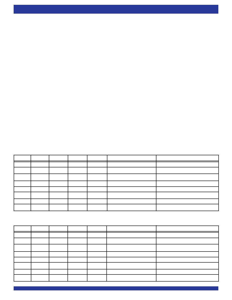
相关PDF资料 |
PDF描述 |
|---|---|
| VE-26F-CU-B1 | CONVERTER MOD DC/DC 72V 200W |
| MX7575JN+ | IC ADC 8BIT MPU COMP 18-DIP |
| VE-26B-CU-B1 | CONVERTER MOD DC/DC 95V 200W |
| MAX1230BEEG+T | IC ADC 12BIT 300KSPS 24-QSOP |
| ISL83385EIAZ | IC 2DRVR/2RCVR RS232 3V 20-SSOP |
相关代理商/技术参数 |
参数描述 |
|---|---|
| IDT723672L12PQF | 功能描述:IC FIFO SYNC 16384X36 132QFP RoHS:否 类别:集成电路 (IC) >> 逻辑 - FIFO 系列:7200 标准包装:15 系列:74F 功能:异步 存储容量:256(64 x 4) 数据速率:- 访问时间:- 电源电压:4.5 V ~ 5.5 V 工作温度:0°C ~ 70°C 安装类型:通孔 封装/外壳:24-DIP(0.300",7.62mm) 供应商设备封装:24-PDIP 包装:管件 其它名称:74F433 |
| IDT723672L15PF | 功能描述:IC FIFO SYNC 16384X36 120QFP RoHS:否 类别:集成电路 (IC) >> 逻辑 - FIFO 系列:7200 标准包装:15 系列:74F 功能:异步 存储容量:256(64 x 4) 数据速率:- 访问时间:- 电源电压:4.5 V ~ 5.5 V 工作温度:0°C ~ 70°C 安装类型:通孔 封装/外壳:24-DIP(0.300",7.62mm) 供应商设备封装:24-PDIP 包装:管件 其它名称:74F433 |
| IDT723672L15PF8 | 功能描述:IC FIFO SYNC 16384X36 120QFP RoHS:否 类别:集成电路 (IC) >> 逻辑 - FIFO 系列:7200 标准包装:15 系列:74F 功能:异步 存储容量:256(64 x 4) 数据速率:- 访问时间:- 电源电压:4.5 V ~ 5.5 V 工作温度:0°C ~ 70°C 安装类型:通孔 封装/外壳:24-DIP(0.300",7.62mm) 供应商设备封装:24-PDIP 包装:管件 其它名称:74F433 |
| IDT723672L15PQF | 功能描述:IC FIFO SYNC 16384X36 132QFP RoHS:否 类别:集成电路 (IC) >> 逻辑 - FIFO 系列:7200 标准包装:15 系列:74F 功能:异步 存储容量:256(64 x 4) 数据速率:- 访问时间:- 电源电压:4.5 V ~ 5.5 V 工作温度:0°C ~ 70°C 安装类型:通孔 封装/外壳:24-DIP(0.300",7.62mm) 供应商设备封装:24-PDIP 包装:管件 其它名称:74F433 |
| IDT723673L12PF | 功能描述:IC FIFO SYNC 8192X36 128QFP RoHS:否 类别:集成电路 (IC) >> 逻辑 - FIFO 系列:7200 标准包装:15 系列:74F 功能:异步 存储容量:256(64 x 4) 数据速率:- 访问时间:- 电源电压:4.5 V ~ 5.5 V 工作温度:0°C ~ 70°C 安装类型:通孔 封装/外壳:24-DIP(0.300",7.62mm) 供应商设备封装:24-PDIP 包装:管件 其它名称:74F433 |
发布紧急采购,3分钟左右您将得到回复。