- 您现在的位置:买卖IC网 > PDF目录9951 > IDT72615L25J8 (IDT, Integrated Device Technology Inc)IC FIFO BY SYNC 512X18X2 68PLCC PDF资料下载
参数资料
| 型号: | IDT72615L25J8 |
| 厂商: | IDT, Integrated Device Technology Inc |
| 文件页数: | 14/17页 |
| 文件大小: | 0K |
| 描述: | IC FIFO BY SYNC 512X18X2 68PLCC |
| 标准包装: | 250 |
| 系列: | 7200 |
| 功能: | 同步 |
| 存储容量: | 18.4K(512 x 18 x 2) |
| 数据速率: | 40MHz |
| 访问时间: | 25ns |
| 电源电压: | 4.5 V ~ 5.5 V |
| 工作温度: | 0°C ~ 70°C |
| 安装类型: | 表面贴装 |
| 封装/外壳: | 68-LCC(J 形引线) |
| 供应商设备封装: | 68-PLCC(24x24) |
| 包装: | 带卷 (TR) |
| 其它名称: | 72615L25J8 |
6
INDUSTRIALTEMPERATURERANGE
IDT72605/72615 CMOS SYNCBiFIFO
256 x 18x 2 and 512 x 18 x 2
CLK
DATA
ADDR, I/0
CONTROL
LOGIC
RAM A
IDT
SYNCBIFIFO
DATA B
CONTROL B
SYSTEM
CLOCK A
CONTROL
LOGIC
CLK
MICROPROCESSOR
A
MICROPROCESSOR
B
DATA
ADDR, I/0
RAM B
SYSTEM
CLOCK B
IDT
SYNCBIFIFO
DATA B
CLKB
CONTROL B
DATA A
CLKA
CONTROL A
DATA A
CONTROL A
2704 drw 05
CLKB
CLKA
FUNCTIONALDESCRIPTION
IDTs SyncBiFIFO is versatile for both multiprocessor and peripheral
applications. Datacanbestoredorretrievedfromtwosourcessimultaneously.
The SyncBiFIFO has registers on all inputs and outputs. Data is only
transferred into the I/O registers on clock edges, hence the interfaces are
synchronous. Two Dual-Port FIFO memory arrays are contained in the
SyncBiFIFO; one data buffer for each direction. Each port has its own
independentclock.DatatransferstotheI/Oregistersaregatedbytheenable
signals. The transfer direction for each port is controlled independently by a
read/writesignal. IndividualoutputenablesignalscontrolwhethertheSyncBiFIFO
is driving the data lines of a port or whether those data lines are in a high-
impedancestate.TheprocessorconnectedtoPortAoftheBiFIFOcansend
orreceivemessagesdirectlytothePortBdeviceusingthe18-bitbypasspath.
The SyncBiFIFO can be used in multiples of 18-bits. In a 36- to 36-bit
configuration, two SyncBiFIFOs operate in parallel. Both devices are pro-
grammedsimultaneously, 18databitstoeachdevice. Thisconfigurationcan
beextendedtowiderbuswidths(54-to54-bits,72-to72-bits,etc.)byadding
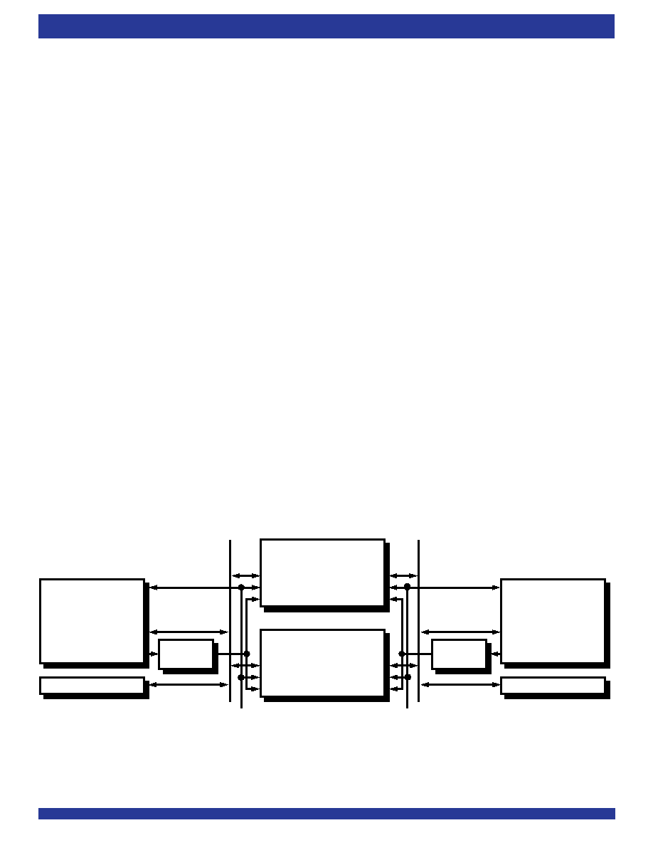
moreSyncBiFIFOstotheconfiguration.Figure1showsmultipleSyncBiFIFOs
configuredfor multiprocessorcommunication.
The microprocessor or microcontroller connected to Port A controls all
operationsoftheSyncBiFIFO.Thus,allPortAinterfacepinsareinputsdriven
by the controlling processor. Port B interfaces with a second processor. The
Port B control pins are inputs driven by the second processor.
RESET
ResetisaccomplishedwhenevertheReset(RS)inputistakentoaLOWstate
with CSA, ENA and ENB HIGH. During reset, both internal read and write
pointersaresettothefirstlocation.Aresetisrequiredafterpowerupbeforea
writeoperationcantakeplace.TheA
→BandB→AFIFOEmptyFlags(EFAB,
EFBA)andProgrammableAlmost-Emptyflags(PAEAB, PAEBA)willbesetto
LOW after tRSF. The A
→B and B→A FIFO Full Flags (FFAB, FFBA) and
ProgrammableAlmost-Fullflags(PAFAB,PAFBA)willbesettoHIGHaftertRSF.
Afterthereset,theoffsetsoftheAlmost-EmptyflagsandAlmost-Fullflagsforthe
A
→BandB→AFIFOoffsetdefaultto8.
PORT A INTERFACE
The SyncBiFIFO is straightforward to use in micro-processor-based
systemsbecauseeachporthasastandardmicroprocessorcontrolset.PortA
interfaceswithmicroprocessorthroughthethreeaddresspins(A2-A0)anda
Chip Select CSA pins. When CSA is asserted, A2,A1,A0 and R/WA are used
to select one of six internal resources (Table 1).
WithA2=0andA1=0,A0determineswhetherdatacanbereadoutofoutput
register or be written into the FIFO (A0=0), or the data can pass through the
FIFO through the bypass path (A0=1).
WithA2=1,fourprogrammableflags(twoA
→BFIFOprogrammableflags
and two B
→A FIFO programmable flags) can be selected: the A→B FIFO
Almost-Empty flag Offset (A1=0, A0=0), A
→B FIFO Almost-Full flag Offset
(A1=0,A0=1),B
→AFIFOAlmost-EmptyflagOffset(A1=1,A0=0),B→AFIFO
Almost-FullflagOffset(A1=1,A0=1).
PortAisdisabledwhenCSAisdeassertedanddataAisinhigh-impedance
state.
BYPASSPATH
ThebypasspathsprovidedirectcommunicationbetweenPortAandPort
B.Therearetwofull18-bitbypasspaths,oneineachdirection.Duringabypass
operation,dataispasseddirectlybetweentheinputandoutputregisters,and
the FIFO memory is undisturbed.
PortAinitiatesandterminatesallbypassoperations. Thebypassflag,BYPB,
isassertedtoinformPortBthatabypassoperationisbeginning.Thebypass
flag state is controlled by the Port A controls, although the BYPB signal is
synchronizedtoCLKB.So,BYPBisassertedonthenextrisingedgeofCLKB
whenA2A1A0=001andCSAisLOW. WhenPortAreturnstonormalFIFOmode
(A2A1A0=000 or CSA is HIGH), BYPB is deasserted on the next CLKB rising
edge.
OncetheSyncBiFIFOisinbypassmode,alldatatransfersarecontrolled
by the standard Port A (R/WA, CLKA, ENA, OEA) and Port B (R/WB, CLKB,
ENB,OEB)interfacepins. Eachbypasspathcanbeconsideredasaoneword
deepFIFO.Dataisheldineachinputregisteruntilitisread. Sincethecontrols
Figure 1. 36- to 36-bit Processor Interface Configuration
NOTES:
1. Upper SyncBiFIFO only is used in 18- to 18-bit configuration.
2. Control A consists of R/WA, ENA, OEA, CSA, A2, A1, A0. Control B consists of R/WB, ENB, OEB.
相关PDF资料 |
PDF描述 |
|---|---|
| V72B36M250BG2 | CONVERTER MOD DC/DC 36V 250W |
| IDT72V3670L6PF8 | IC FIFO SS 8192X36 6NS 128-TQFP |
| IDT72V3670L6BB8 | IC FIFO SS 8192X36 6NS 144-BGA |
| V72B36M250BG | CONVERTER MOD DC/DC 36V 250W |
| IDT72T1865L5BB | IC FIFO 8192X18 5NS 144BGA |
相关代理商/技术参数 |
参数描述 |
|---|---|
| IDT72615L25PF | 功能描述:IC FIFO BY SYNC 512X18X2 64QFP RoHS:否 类别:集成电路 (IC) >> 逻辑 - FIFO 系列:7200 标准包装:15 系列:74F 功能:异步 存储容量:256(64 x 4) 数据速率:- 访问时间:- 电源电压:4.5 V ~ 5.5 V 工作温度:0°C ~ 70°C 安装类型:通孔 封装/外壳:24-DIP(0.300",7.62mm) 供应商设备封装:24-PDIP 包装:管件 其它名称:74F433 |
| IDT72615L25PF8 | 功能描述:IC FIFO BY SYNC 512X18X2 64QFP RoHS:否 类别:集成电路 (IC) >> 逻辑 - FIFO 系列:7200 标准包装:90 系列:7200 功能:同步 存储容量:288K(16K x 18) 数据速率:100MHz 访问时间:10ns 电源电压:4.5 V ~ 5.5 V 工作温度:0°C ~ 70°C 安装类型:表面贴装 封装/外壳:64-LQFP 供应商设备封装:64-TQFP(14x14) 包装:托盘 其它名称:72271LA10PF |
| IDT72615L35J | 功能描述:IC FIFO BY SYNC 512X18X2 68PLCC RoHS:否 类别:集成电路 (IC) >> 逻辑 - FIFO 系列:7200 标准包装:15 系列:74F 功能:异步 存储容量:256(64 x 4) 数据速率:- 访问时间:- 电源电压:4.5 V ~ 5.5 V 工作温度:0°C ~ 70°C 安装类型:通孔 封装/外壳:24-DIP(0.300",7.62mm) 供应商设备封装:24-PDIP 包装:管件 其它名称:74F433 |
| IDT72615L35J8 | 功能描述:IC FIFO BY SYNC 512X18X2 68PLCC RoHS:否 类别:集成电路 (IC) >> 逻辑 - FIFO 系列:7200 标准包装:90 系列:7200 功能:同步 存储容量:288K(16K x 18) 数据速率:100MHz 访问时间:10ns 电源电压:4.5 V ~ 5.5 V 工作温度:0°C ~ 70°C 安装类型:表面贴装 封装/外壳:64-LQFP 供应商设备封装:64-TQFP(14x14) 包装:托盘 其它名称:72271LA10PF |
| IDT72615L35PF | 功能描述:IC FIFO BY SYNC 512X18X2 64QFP RoHS:否 类别:集成电路 (IC) >> 逻辑 - FIFO 系列:7200 标准包装:15 系列:74F 功能:异步 存储容量:256(64 x 4) 数据速率:- 访问时间:- 电源电压:4.5 V ~ 5.5 V 工作温度:0°C ~ 70°C 安装类型:通孔 封装/外壳:24-DIP(0.300",7.62mm) 供应商设备封装:24-PDIP 包装:管件 其它名称:74F433 |
发布紧急采购,3分钟左右您将得到回复。