- 您现在的位置:买卖IC网 > PDF目录10043 > IDT72811L25TFI (IDT, Integrated Device Technology Inc)IC FIFO SYNC DUAL 512X9 64QFP PDF资料下载
参数资料
| 型号: | IDT72811L25TFI |
| 厂商: | IDT, Integrated Device Technology Inc |
| 文件页数: | 10/16页 |
| 文件大小: | 0K |
| 描述: | IC FIFO SYNC DUAL 512X9 64QFP |
| 标准包装: | 80 |
| 系列: | 7200 |
| 功能: | 同步 |
| 存储容量: | 4.6K(512 x 9) |
| 数据速率: | 40MHz |
| 访问时间: | 25ns |
| 电源电压: | 4.5 V ~ 5.5 V |
| 工作温度: | -40°C ~ 85°C |
| 安装类型: | 表面贴装 |
| 封装/外壳: | 64-LQFP |
| 供应商设备封装: | 64-TQFP(10x10) |
| 包装: | 托盘 |
| 其它名称: | 72811L25TFI |
3
IDT72801/728211/72821/72831/72841/72851 DUAL CMOS SyncFIFOTM
DUAL 256 x 9, DUAL 512 x 9, DUAL 1K x 9, DUAL 2K x 9, DUAL 4K x 9, DUAL 8K x 9
COMMERCIAL AND INDUSTRIAL
TEMPERATURERANGES
MARCH 2013
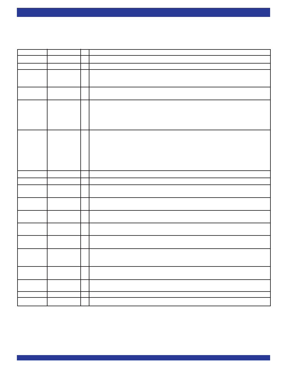
Symbol
Name
I/O
Description
DA0-DA8
ADataInputs
I
9-bit data inputs to RAM array A.
DB0-DB8
BDataInputs
I
9-bit data inputs to RAM array B.
RSA
, RSB
Reset
I
When RSA (RSB) is set LOW, the associated internal read and write pointers of array A (B) are set to
the first location; FFA (FFB) and PAFA (PAFB) go HIGH, and PAEA (PAEB) and EFA (EFB) go
LOW. After power-up, a reset of both FIFOs A and B is required before an initial Write.
WCLKA
WriteClock
I
Data is written into the FIFO A (B) on a LOW-to-HIGH transition of WCLKA (WCLKB) when the write
WCLKB
enable(s) are asserted.
WENA1
WriteEnable1
I
If FIFO A (B) is configured to have programmable flags, WENA1 (WENB1) is the only Write
WENB1
Enable pin that can be used. When WENA1 (WENB1) is LOW, data A (B) is written into the FIFO
on every LOW-to-HIGH transition WCLKA (WCLKB). If the FIFO is configured to have two write enables,
WENA1
(WENB1) must be LOW and WENA2 (WENB2) must be HIGH to write data into the FIFO. Data
will not be written into the FIFO if FFA (FFB) is LOW.
WENA2/LDA
WriteEnable2/
I
FIFO A (B) is configured at reset to have either two write enables or programmable flags. If LDA (LDB)
WENB2/LDB
Load
is HIGH at reset, this pin operates as a second write enable. If WENA2/LDA (WENB2/LDB) is LOW
at reset this pin operates as a control to load and read the programmable flag offsets for its respective array.
If the FIFO is configured to have two write enables, WENA1 (WENB1) must be LOW
and WENA2 (WENB2) must be HIGH to write data into FIFO A (B). Data will not be written into FIFO A (B)
if FFA (FFB) is LOW. If the FIFO is configured to have programmable flags, LDA (LDB) is held LOW to write or
readtheprogrammableflagoffsets.
QA0-QA8
ADataOutputs
O
9-bit data outputs from RAM array A.
QB0-QB8
BDataOutputs
O
9-bit data outputs from RAM array B.
RCLKA
Read Clock
I
Data is read from FIFO A (B) on a LOW-to-HIGH transition of RCLKA (RCLKB) when RENA1
RCLKB
(RENB1) and RENA2 (RENB2) are asserted.
RENA1
Read Enable 1
I
When RENA1 (RENB1) and RENA2 (RENB2) are LOW, data is read from FIFO A (B) on every
RENB1
LOW-to-HIGH transition of RCLKA (RCLKB). Data will not be read from Array A (B) if EFA (EFB) is LOW.
RENA2
Read Enable 2
I
When RENA1 (RENB1) and RENA2 (RENB2) are LOW, data is read from the FIFO A (B) on every
RENB2
LOW-to-HIGH transition of RCLKA (RCLKB). Data will not be read from array A (B) if the EFA(EFB) is LOW.
OEA
OutputEnable
I
When OEA (OEB) is LOW, outputs DA0-DA8 (DB0-DB8) are active. If OEA (OEB) is HIGH, the
OEB
outputs DA0-DA8 (DB0-DB8) will be in a high-impedance state.
EFA
EmptyFlag
O
When EFA (EFB) is LOW, FIFO A (B) is empty and further data reads from the output are inhibited.
EFB
When EFA (EFB) is HIGH, FIFO A (B) is not empty. EFA (EFB) is synchronized to RCLKA (RCLKB).
PAEA
Programmable
O
When PAEA (PAEB) is LOW, FIFO A (B) is almost-empty based on the offset programmed into the
PAEB
Almost-Empty
appropriate offset register. The default offset at reset is Empty+7. PAEA(PAEB) is synchronized to
Flag
RCLKA (RCLKB).
PAFA
Programmable
O
When PAFA(PAFB) is LOW, FIFO A (B) is almost-full based on the offset programmed into the appropriate
PAFB
Almost-FullFlag
offset register. The default offset at reset is Full-7. PAFA(PAFB) is synchronized to WCLKA (WCLKB).
FFA
Full Flag
O
When FFA (FFB) is LOW, FIFO A (B) is full and further data writes into the input are inhibited.
FFB
When FFA (FFB) is HIGH, FIFO A (B) is not full. FFA (FFB) is synchronized to WCLKA (WCLKB).
VCC
Power
+5V power supply pin.
GND
Ground
0V ground pin.
PIN DESCRIPTIONS
The IDT72801/72811/72821/72831/72841/72851s two FIFOs, referred
to as FIFO A and FIFO B, are identical in every respect. The following
description defines the input and output signals for FIFO A. The correspond-
ing signal names for FIFO B are provided in parentheses.
相关PDF资料 |
PDF描述 |
|---|---|
| LTC2207IUK-14#TRPBF | IC ADC 14BIT 105MSPS 48-QFN |
| MS3108E20-11P | CONN PLUG 13POS RT ANG W/PINS |
| IDT72811L15TF | IC FIFO SYNC DUAL 512X9 64QFP |
| VI-2VX-MY | CONVERTER MOD DC/DC 5.2V 50W |
| LT1134AIN#PBF | IC 4DRV/4RCV RS232 5V 24-DIP |
相关代理商/技术参数 |
参数描述 |
|---|---|
| IDT72811L25TFI8 | 功能描述:IC FIFO SYNC DUAL 512X9 64QFP RoHS:否 类别:集成电路 (IC) >> 逻辑 - FIFO 系列:7200 标准包装:80 系列:7200 功能:同步 存储容量:18.4K(1K x 18) 数据速率:- 访问时间:10ns 电源电压:4.5 V ~ 5.5 V 工作温度:0°C ~ 70°C 安装类型:表面贴装 封装/外壳:64-LQFP 供应商设备封装:64-TQFP(10x10) 包装:托盘 其它名称:72225LB10TF |
| IDT72815LB10PF | 功能描述:IC FIFO SYNC DUAL 512X18 128TQFP RoHS:否 类别:集成电路 (IC) >> 逻辑 - FIFO 系列:7200 标准包装:90 系列:7200 功能:同步 存储容量:288K(16K x 18) 数据速率:100MHz 访问时间:10ns 电源电压:4.5 V ~ 5.5 V 工作温度:0°C ~ 70°C 安装类型:表面贴装 封装/外壳:64-LQFP 供应商设备封装:64-TQFP(14x14) 包装:托盘 其它名称:72271LA10PF |
| IDT72815LB10PF8 | 功能描述:IC FIFO SYNC DUAL 512X18 128TQFP RoHS:否 类别:集成电路 (IC) >> 逻辑 - FIFO 系列:7200 标准包装:90 系列:7200 功能:同步 存储容量:288K(16K x 18) 数据速率:100MHz 访问时间:10ns 电源电压:4.5 V ~ 5.5 V 工作温度:0°C ~ 70°C 安装类型:表面贴装 封装/外壳:64-LQFP 供应商设备封装:64-TQFP(14x14) 包装:托盘 其它名称:72271LA10PF |
| IDT72815LB15BG | 功能描述:IC FIFO SYNC DUAL 512X18 121BGA RoHS:否 类别:集成电路 (IC) >> 逻辑 - FIFO 系列:7200 标准包装:15 系列:74F 功能:异步 存储容量:256(64 x 4) 数据速率:- 访问时间:- 电源电压:4.5 V ~ 5.5 V 工作温度:0°C ~ 70°C 安装类型:通孔 封装/外壳:24-DIP(0.300",7.62mm) 供应商设备封装:24-PDIP 包装:管件 其它名称:74F433 |
| IDT72815LB15BG8 | 功能描述:IC FIFO SYNC DUAL 512X18 121BGA RoHS:否 类别:集成电路 (IC) >> 逻辑 - FIFO 系列:7200 标准包装:15 系列:74F 功能:异步 存储容量:256(64 x 4) 数据速率:- 访问时间:- 电源电压:4.5 V ~ 5.5 V 工作温度:0°C ~ 70°C 安装类型:通孔 封装/外壳:24-DIP(0.300",7.62mm) 供应商设备封装:24-PDIP 包装:管件 其它名称:74F433 |
发布紧急采购,3分钟左右您将得到回复。