- 您现在的位置:买卖IC网 > PDF目录10068 > IDT72V235L10PF8 (IDT, Integrated Device Technology Inc)IC FIFO SYNC 2048X18 10NS 64TQFP PDF资料下载
参数资料
| 型号: | IDT72V235L10PF8 |
| 厂商: | IDT, Integrated Device Technology Inc |
| 文件页数: | 25/25页 |
| 文件大小: | 0K |
| 描述: | IC FIFO SYNC 2048X18 10NS 64TQFP |
| 标准包装: | 750 |
| 系列: | 72V |
| 功能: | 同步 |
| 存储容量: | 36.8K(2K x 18) |
| 数据速率: | 100MHz |
| 访问时间: | 10ns |
| 电源电压: | 3 V ~ 3.6 V |
| 工作温度: | 0°C ~ 70°C |
| 安装类型: | 表面贴装 |
| 封装/外壳: | 64-LQFP |
| 供应商设备封装: | 64-TQFP(14x14) |
| 包装: | 带卷 (TR) |
| 其它名称: | 72V235L10PF8 |
9
IDT72V205/72V215/72V225/72V235/72V245 3.3V CMOS SyncFIFOTM
256 x 18, 512 x 18, 1,024 x 18, 2,048 x 18 and 4,096 x 18
COMMERCIALANDINDUSTRIAL
TEMPERATURERANGES
MARCH 2013
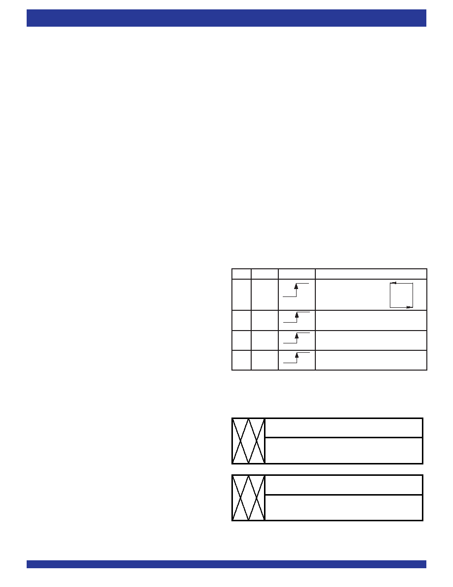
Figure 2. Writing to Offset Registers
LD
WEN
WCLK
Selection
0
Writingtooffsetregisters:
EmptyOffset
FullOffset
0
1
NoOperation
1
0
Write Into FIFO
1
NoOperation
Figure 3. Offset Register Location and Default Values
SIGNAL DESCRIPTIONS:
INPUTS:
DATA IN (D0 - D17)
Data inputs for 18-bit wide data.
CONTROLS:
RESET (RS)
Reset is accomplished whenever the Reset (RS) input is taken to a LOW
state. During reset, both internal read and write pointers are set to the first
location. A reset is required after power-up before a write operation can take
place.TheHalf-FullFlag(HF)andProgrammableAlmost-FullFlag(PAF)will
beresettoHIGHaftertRSF.TheProgrammableAlmost-EmptyFlag(PAE)will
be reset to LOW after tRSF. The Full Flag (FF) will reset to HIGH. The Empty
Flag(EF)willresettoLOWinIDTStandardmodebutwillresettoHIGHinFWFT
mode. Duringreset,theoutputregisterisinitializedtoallzerosandtheoffset
registersareinitializedtotheirdefaultvalues.
WRITE CLOCK (WCLK)
AwritecycleisinitiatedontheLOW-to-HIGHtransitionoftheWriteClock
(WCLK).DatasetupandholdtimesmustbemetwithrespecttotheLOW-to-HIGH
transitionofWCLK.
The Write and Read Clocks can be asynchronous or coincident.
WRITE ENABLE (WEN)
WhentheWENinput isLOW,datamaybeloadedintotheFIFORAMarray
on the rising edge of every WCLK cycle if the device is not full. Data is stored
in the RAM array sequentially and independently of any ongoing read
operation.
WhenWENisHIGH,nonewdataiswrittenintheRAMarrayoneachWCLK
cycle.
To prevent data overflow in the IDT Standard Mode, FF will go LOW,
inhibiting further write operations. Upon the completion of a valid read cycle,
FF will go HIGH allowing a write to occur. TheFF flag is updated on the rising
edgeofWCLK.
To prevent data overflow in the FWFT mode, IR will go HIGH, inhibiting
further write operations. Upon the completion of a valid read cycle, IR will go
LOWallowingawritetooccur. TheIRflagisupdatedontherisingedgeofWCLK.
WENisignoredwhentheFIFOisfullineitherFWFTorIDTStandardmode.
READ CLOCK (RCLK)
DatacanbereadontheoutputsontheLOW-to-HIGHtransitionoftheRead
Clock (RCLK), when Output Enable (OE) is set LOW.
The Write and Read Clocks can be asynchronous or coincident.
READ ENABLE (REN)
WhenReadEnableisLOW,dataisloadedfromtheRAMarrayintotheoutput
register on the rising edge of every RCLK cycle if the device is not empty.
WhentheRENinputisHIGH,theoutputregisterholdsthepreviousdataand
nonewdataisloadedintotheoutputregister. ThedataoutputsQ0-Qnmaintain
the previous data value.
In the IDT Standard mode, every word accessed at Qn, including the first
wordwrittentoanemptyFIFO,mustberequestedusingREN. Whenthelast
wordhasbeenreadfromtheFIFO,theEmptyFlag(EF)willgoLOW,inhibiting
furtherreadoperations. RENisignoredwhentheFIFOisempty. Onceawrite
isperformed,EFwillgoHIGHallowingareadtooccur. TheEFflagisupdated
on the rising edge of RCLK.
IntheFWFTmode,thefirstwordwrittentoanemptyFIFOautomaticallygoes
to the outputs Qn, on the third valid LOW to HIGH transition of RCLK + tSKEW
afterthefirstwrite. RENdoesnotneedtobeassertedLOW. Inordertoaccess
allotherwords,areadmustbeexecutedusingREN. TheRCLKLOWtoHIGH
transitionafterthelastwordhasbeenreadfromtheFIFO,OutputReady(OR)
willgoHIGHwithatrue read(RCLKwith REN=LOW),inhibitingfurtherread
operations. REN is ignored when the FIFO is empty.
OUTPUT ENABLE (OE)
When Output Enable (OE) is enabled (LOW), the parallel output buffers
receivedatafromtheoutputregister.WhenOEisdisabled(HIGH),theQoutput
databusisinahigh-impedancestate.
LOAD (LD)
The IDT72V205/72V215/72V225/72V235/72V245 devices contain two
12-bitoffsetregisterswithdataontheinputs,orreadontheoutputs. Whenthe
Load (LD) pin is set LOW and WEN is set LOW, data on the inputs D0-D11 is
writtenintotheEmptyOffsetregisteronthefirstLOW-to-HIGHtransitionofthe
Write Clock (WCLK). When the LD pin and WEN are held LOW then data is
written into the Full Offset register on the second LOW-to-HIGH transition of
WCLK.ThethirdtransitionofWCLKagainwritestotheEmptyOffsetregister.
However,writingalloffsetregistersdoesnothavetooccuratonetime.One
ortwooffsetregisterscanbewrittenandthenbybringingtheLDpinHIGH,the
FIFOisreturnedtonormalread/writeoperation.WhentheLDpinissetLOW,
and WEN is LOW, the next offset register in sequence is written.
EMPTY OFFSET REGISTER
17
11
0
001FH (72V205) 003FH (72V215):
007FH (72V225/72V235/72V245)
FULL OFFSET REGISTER
17
11
0
DEFAULT VALUE
001FH (72V205) 003FH (72V215):
007FH (72V225/72V235/72V245)
4294 drw 04
NOTE:
1. Any bits of the offset register not being programmed should be set to zero.
NOTE:
1. The same selection sequence applies to reading from the registers. REN is enabled and
read is performed on the LOW-to-HIGH transition of RCLK.
相关PDF资料 |
PDF描述 |
|---|---|
| AD1674AD | IC ADC SNGL 12BIT 28-CDIP |
| MS27468E9B6S | CONN RCPT 6POS JAM NUT W/SCKT |
| LT1080IN#PBF | IC DRVR/RCVR DUAL-RS232 5V 18DIP |
| AD976BRSZ | IC ADC 16BIT 100KSPS 28SSOP |
| AD976AARZ | IC ADC 16BIT 200KSPS 28-SOIC |
相关代理商/技术参数 |
参数描述 |
|---|---|
| IDT72V235L10PFG | 功能描述:IC FIFO SYNC 2048X18 10NS 64TQFP RoHS:是 类别:集成电路 (IC) >> 逻辑 - FIFO 系列:72V 标准包装:90 系列:7200 功能:同步 存储容量:288K(16K x 18) 数据速率:100MHz 访问时间:10ns 电源电压:4.5 V ~ 5.5 V 工作温度:0°C ~ 70°C 安装类型:表面贴装 封装/外壳:64-LQFP 供应商设备封装:64-TQFP(14x14) 包装:托盘 其它名称:72271LA10PF |
| IDT72V235L10PFG8 | 功能描述:IC FIFO SYNC 2048X18 10NS 64TQFP RoHS:是 类别:集成电路 (IC) >> 逻辑 - FIFO 系列:72V 标准包装:80 系列:7200 功能:同步 存储容量:18.4K(1K x 18) 数据速率:- 访问时间:10ns 电源电压:4.5 V ~ 5.5 V 工作温度:0°C ~ 70°C 安装类型:表面贴装 封装/外壳:64-LQFP 供应商设备封装:64-TQFP(10x10) 包装:托盘 其它名称:72225LB10TF |
| IDT72V235L10TF | 功能描述:IC FIFO SYNC 2048X18 10NS 64QFP RoHS:否 类别:集成电路 (IC) >> 逻辑 - FIFO 系列:72V 标准包装:90 系列:7200 功能:同步 存储容量:288K(16K x 18) 数据速率:100MHz 访问时间:10ns 电源电压:4.5 V ~ 5.5 V 工作温度:0°C ~ 70°C 安装类型:表面贴装 封装/外壳:64-LQFP 供应商设备封装:64-TQFP(14x14) 包装:托盘 其它名称:72271LA10PF |
| IDT72V235L10TF8 | 功能描述:IC FIFO SYNC 2048X18 10NS 64QFP RoHS:否 类别:集成电路 (IC) >> 逻辑 - FIFO 系列:72V 标准包装:80 系列:7200 功能:同步 存储容量:18.4K(1K x 18) 数据速率:- 访问时间:10ns 电源电压:4.5 V ~ 5.5 V 工作温度:0°C ~ 70°C 安装类型:表面贴装 封装/外壳:64-LQFP 供应商设备封装:64-TQFP(10x10) 包装:托盘 其它名称:72225LB10TF |
| IDT72V235L10TFG | 功能描述:IC FIFO 2048X18 SYNC 64TQFP RoHS:是 类别:集成电路 (IC) >> 逻辑 - FIFO 系列:72V 标准包装:90 系列:7200 功能:同步 存储容量:288K(16K x 18) 数据速率:100MHz 访问时间:10ns 电源电压:4.5 V ~ 5.5 V 工作温度:0°C ~ 70°C 安装类型:表面贴装 封装/外壳:64-LQFP 供应商设备封装:64-TQFP(14x14) 包装:托盘 其它名称:72271LA10PF |
发布紧急采购,3分钟左右您将得到回复。