- 您现在的位置:买卖IC网 > PDF目录9951 > IDT72V3670L6BB8 (IDT, Integrated Device Technology Inc)IC FIFO SS 8192X36 6NS 144-BGA PDF资料下载
参数资料
| 型号: | IDT72V3670L6BB8 |
| 厂商: | IDT, Integrated Device Technology Inc |
| 文件页数: | 39/46页 |
| 文件大小: | 0K |
| 描述: | IC FIFO SS 8192X36 6NS 144-BGA |
| 标准包装: | 1,000 |
| 系列: | 72V |
| 功能: | 异步,同步 |
| 存储容量: | 288K(8K x 36) |
| 数据速率: | 166MHz |
| 访问时间: | 4ns |
| 电源电压: | 3.15 V ~ 3.45 V |
| 工作温度: | 0°C ~ 70°C |
| 安装类型: | 表面贴装 |
| 封装/外壳: | 144-BGA |
| 供应商设备封装: | 144-PBGA(13x13) |
| 包装: | 带卷 (TR) |
| 其它名称: | 72V3670L6BB8 |
第1页第2页第3页第4页第5页第6页第7页第8页第9页第10页第11页第12页第13页第14页第15页第16页第17页第18页第19页第20页第21页第22页第23页第24页第25页第26页第27页第28页第29页第30页第31页第32页第33页第34页第35页第36页第37页第38页当前第39页第40页第41页第42页第43页第44页第45页第46页
44
COMMERCIAL AND INDUSTRIAL
TEMPERATURE RANGES
IDT72V3640/50/60/70/80/90 3.3V HIGH DENSITY SUPERSYNC IITM 36-BIT FIFO
1,024 x 36, 2,048 x 36, 4,096 x 36, 8,192 x 36, 16,384 x 36 and 32,768 x 36
OCTOBER 22, 2008
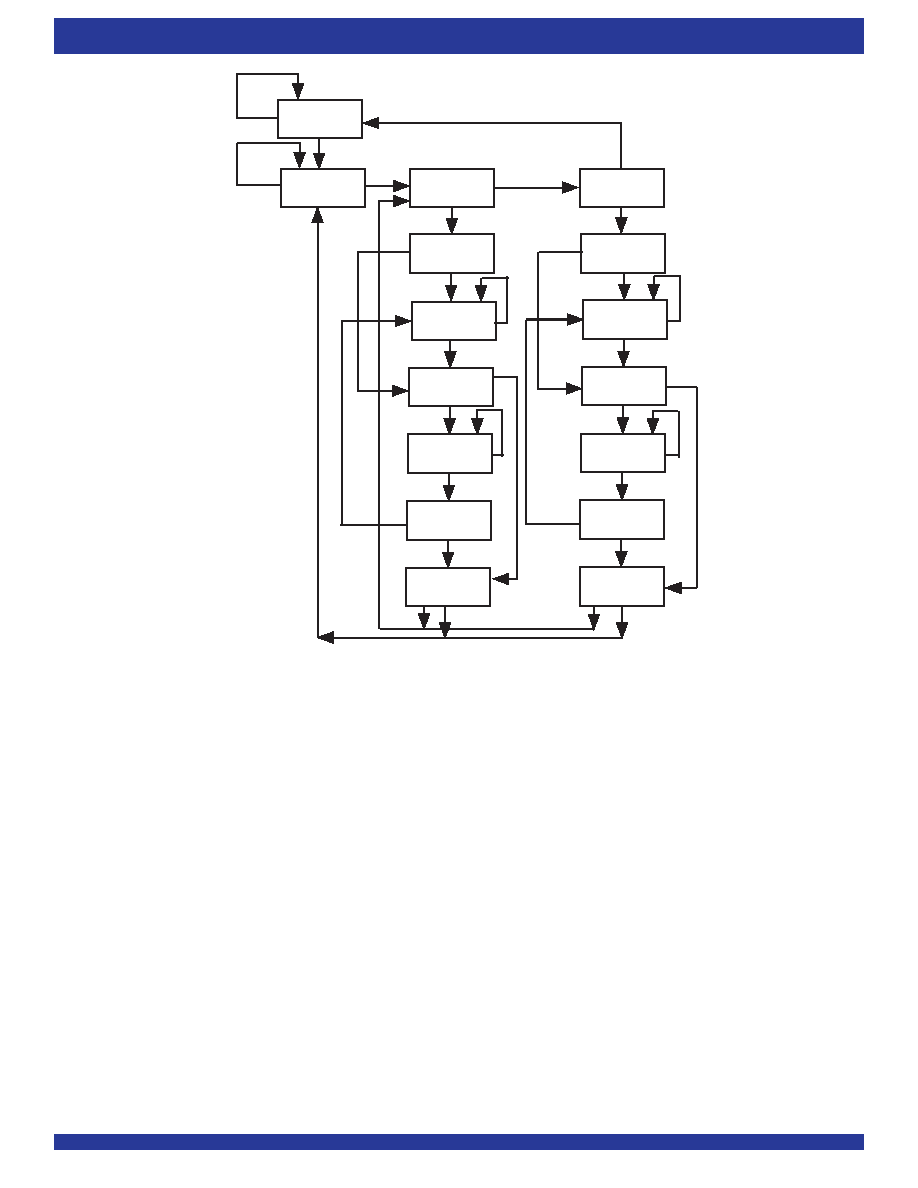
Figure 33. TAP Controller State Diagram
Test-Logic
Reset
Run-Test/
Idle
1
0
Select-
DR-Scan
Select-
IR-Scan
1
Capture-IR
0
Capture-DR
0
EXit1-DR
1
Pause-DR
0
Exit2-DR
1
Update-DR
1
Exit1-IR
1
Exit2-IR
1
Update-IR
1
0
1
4667 drw38
0
Shift-DR
0
Shift-IR
0
Pause-IR
0
1
Input = TMS
0
1
Refer to the IEEE Standard Test Access Port Specification (IEEE Std.
1149.1) for the full state diagram
All state transitions within the TAP controller occur at the rising edge of the
TCLK pulse. The TMS signal level (0 or 1) determines the state progression
that occurs on each TCLK rising edge. The TAP controller takes precedence
over the FIFO memory and must be reset after power up of the device. See
TRST description for more details on TAP controller reset.
CAPTURE-DR
Data is loaded from the parallel input pins or core outputs into the Data
Register.
SHIFT-DR
Thepreviouslycaptureddataisshiftedinserially,LSBfirstattherisingedge
ofTCLKintheTDI/TDOpathandshiftedoutserially,LSBfirstatthefallingedge
of TCLK towards the output.
UPDATE-DR
The shifting process has been completed. The data is latched into their
parallel outputs in this state to be accessed through the internal bus.
EXIT1-DR / EXIT2-DR
Thisisatemporarycontrollerstate.IfTMSisheldhigh,arisingedgeapplied
toTCKwhileinthisstatecausesthecontrollertoentertheUpdate-DRstate.This
terminates the scanning process. All test data registers selected by the current
instruction retain their previous state unchanged.
PAUSE-DR
This controller state allows shifting of the test data register in the serial path
between TDI and TDO to be temporarily halted. All test data registers selected
by the current instruction retain their previous state unchanged.
Capture-IR, Shift-IR and Update-IR, Exit-IR and Pause-IR are
similartoDataregisters.Theseinstructionsoperateontheinstructionregisters.
NOTES:
1. Five consecutive TCK cycles with TMS = 1 will reset the TAP.
2. TAP controller does not automatically reset upon power-up. The user must provide a reset to the TAP controller (either by
TRST or TMS).
3. TAP controller must be reset before normal FIFO operations can begin.
相关PDF资料 |
PDF描述 |
|---|---|
| V72B36M250BG | CONVERTER MOD DC/DC 36V 250W |
| IDT72T1865L5BB | IC FIFO 8192X18 5NS 144BGA |
| HIN232CBZ-T | IC 2DRVR/2RCVR RS232 5V 16-SOIC |
| HIN202IBNZ | IC 2DRVR/2RCVR RS232 5V 16-SOIC |
| VI-21K-MX-F4 | CONVERTER MOD DC/DC 40V 75W |
相关代理商/技术参数 |
参数描述 |
|---|---|
| IDT72V3670L6PF | 功能描述:IC FIFO SS 8192X36 6NS 128-TQFP RoHS:否 类别:集成电路 (IC) >> 逻辑 - FIFO 系列:72V 标准包装:15 系列:74F 功能:异步 存储容量:256(64 x 4) 数据速率:- 访问时间:- 电源电压:4.5 V ~ 5.5 V 工作温度:0°C ~ 70°C 安装类型:通孔 封装/外壳:24-DIP(0.300",7.62mm) 供应商设备封装:24-PDIP 包装:管件 其它名称:74F433 |
| IDT72V3670L6PF8 | 功能描述:IC FIFO SS 8192X36 6NS 128-TQFP RoHS:否 类别:集成电路 (IC) >> 逻辑 - FIFO 系列:72V 标准包装:15 系列:74F 功能:异步 存储容量:256(64 x 4) 数据速率:- 访问时间:- 电源电压:4.5 V ~ 5.5 V 工作温度:0°C ~ 70°C 安装类型:通孔 封装/外壳:24-DIP(0.300",7.62mm) 供应商设备封装:24-PDIP 包装:管件 其它名称:74F433 |
| IDT72V3670L6PFG | 功能描述:IC FIFO 8192X36 SYNC 6NS 128TQFP RoHS:是 类别:集成电路 (IC) >> 逻辑 - FIFO 系列:72V 标准包装:15 系列:74F 功能:异步 存储容量:256(64 x 4) 数据速率:- 访问时间:- 电源电压:4.5 V ~ 5.5 V 工作温度:0°C ~ 70°C 安装类型:通孔 封装/外壳:24-DIP(0.300",7.62mm) 供应商设备封装:24-PDIP 包装:管件 其它名称:74F433 |
| IDT72V3670L6PFG8 | 制造商:Integrated Device Technology Inc 功能描述:IC FIFO SS 8192X36 6NS 128-TQFP |
| IDT72V3670L7-5BB | 功能描述:IC FIFO SS 8192X36 7-5NS 144BGA RoHS:否 类别:集成电路 (IC) >> 逻辑 - FIFO 系列:72V 标准包装:15 系列:74F 功能:异步 存储容量:256(64 x 4) 数据速率:- 访问时间:- 电源电压:4.5 V ~ 5.5 V 工作温度:0°C ~ 70°C 安装类型:通孔 封装/外壳:24-DIP(0.300",7.62mm) 供应商设备封装:24-PDIP 包装:管件 其它名称:74F433 |
发布紧急采购,3分钟左右您将得到回复。