- 您现在的位置:买卖IC网 > PDF目录9188 > IDT72V70810TF8 (IDT, Integrated Device Technology Inc)IC DGTL SW 1024X1024 64-STQFP PDF资料下载
参数资料
| 型号: | IDT72V70810TF8 |
| 厂商: | IDT, Integrated Device Technology Inc |
| 文件页数: | 16/22页 |
| 文件大小: | 0K |
| 描述: | IC DGTL SW 1024X1024 64-STQFP |
| 标准包装: | 1,250 |
| 系列: | 72V |
| 类型: | 多路复用器 |
| 电路: | 1 x 8:8 |
| 独立电路: | 1 |
| 电压电源: | 单电源 |
| 电源电压: | 3 V ~ 3.6 V |
| 工作温度: | -40°C ~ 85°C |
| 安装类型: | 表面贴装 |
| 封装/外壳: | 64-LQFP |
| 供应商设备封装: | 64-TQFP(10x10) |
| 包装: | 带卷 (TR) |
| 其它名称: | 72V70810TF8 |
3
COMMERCIALTEMPERATURERANGE
IDT72V70810 3.3V TIME SLOT INTERCHANGE
DIGITAL SWITCH 1,024 x 1,024
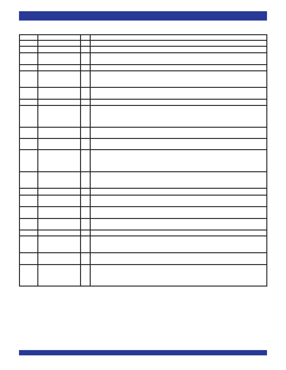
PIN DESCRIPTION
SYMBOL
NAME
I/O
DESCRIPTION
GND
Ground.
Ground Rail.
Vcc
+3.3 Volt Power Supply.
TX0-7
TX Output 0 to 7
O
Serial data output stream. These streams have a data rate of 8.192 Mb/s.
(Three-state Outputs)
RX0-7
RX Input 0 to 7
I
Serial data input stream. These streams have a data rate of 8.192 Mb/s.
F0i
Frame Pulse
I
When the WFPS pin is LOW, this input accepts and automatically identifies frame synchronization signals formatted
according to ST-BUS and GCI specifications. When the WFPS pin is HIGH, this pin accepts a negative frame
pulse which conforms to WFPS formats.
FE/HCLK Frame Evaluation/
I
When the WFPS pin is LOW, this pin is the frame measurement input. When the WFPS pin is HIGH, the HCLK
HCLK Clock
(4.096 MHz clock) is required for frame alignment in the wide frame pulse (WFP) mode.
CLK
Clock
I
Serial clock for shifting data in/out on the serial streams (RX/TX 0-7). This input accepts a 16.384 MHz clock.
RESET
Device Reset
I
This input (active LOW) puts the IDT72V70810 in its reset state that clears the device internal counters, registers
(Schmitt Trigger Input)
and brings TX0-7 and microport data outputs to a high-impedance state. The time constant for a power
up reset circuit must be a minimum of five times the rise time of the power supply. In normal operation, the
RESET pin must be held LOW for a minimum of 100ns to reset the device.
WFPS
Wide Frame
I
When 1, enables the wide frame pulse (WFP) Frame Alignment interface. When 0, the device operates in
Pulse Select
ST-BUS/GCI mode.
A0-7
Address 0-7
I
When non-multiplexed CPU bus operation is selected, these lines provide the A0-A7 address lines to the internal
memories.
DS/
RD
Data Strobe/Read
I
For Motorola multiplexed bus operation, this input is DS. This active HIGH DS input works in conjunction with
CS
to enable the read and write operations. For Motorola non-multiplexed CPU bus operation, this input is DS. This
active LOW input works in conjunction with
CS to enable the read and write operations. For Intel multiplexed bus
operation, this input is
RD. This active LOW input sets the data bus lines (AD0-7, D8-15) as outputs.
R/
W / WR Read/Write / Write
I
In the cases of Motorola non-multiplexed and multiplexed bus operations, this input is R/
W. This input controls
the direction of the data bus lines (AD0-7, D8-15) during a microprocessor access. For Intel multiplexed bus
operation, this input is
WR. This active LOW input is used with RD to control the data bus (AD0-7) lines as inputs.
CS
Chip Select
I
Active LOW input used by a microprocessor to activate the microprocessor port of IDT72V70810.
AS/ALE
Address Strobe or
I
This input is used if multiplexed bus operation is selected via the IM input pin. For Motorola non-multiplexed
Latch Enable
bus operation, connect this pin to ground.
IM
CPU Interface Mode
I
When IM is HIGH, the microprocessor port is in the multiplexed mode. When IM is LOW, the microprocessor
port is in non-multiplexed mode.
AD0-7
Address/Data Bus 0 to 7 I/O
These pins are the eight least significant data bits of the microprocessor port. In multiplexed mode, these pins
are also the input address bits of the microprocessor port.
D8-15
Data Bus 8-15
I/O
These pins are the eight most significant data bits of the microprocessor port.
DTA
Data Transfer
O
This active LOW output signal indicates that a data bus transfer is complete. When the bus cycle ends, this pin
Acknowledgment
drives HIGH and then goes high-impedance, allowing for faster bus cycles with a weaker pull-up resistor. A
pull-up resistor is required to hold a HIGH level when the pin is in high-impedance.
CCO
Control Output
O
This is a 16.384 Mb/s output containing 2.048 bits per frame respectively. The level of each bit is determined
by the CCO bit in the connection memory. See External Drive Control Section.
ODE
Output Drive Enable
I
This is the output enable control for the TX0 to TX7 serial outputs. When ODE input is LOW and the OSB
bit of the IMS register is LOW, TX0-7 are in a high-impedance state. If this input is HIGH, the TX0-7
output drivers are enabled. However, each channel may still be put into a high-impedance state by using
the per channel control bit in the connection memory.
相关PDF资料 |
PDF描述 |
|---|---|
| MS3450W22-6SW | CONN RCPT 3POS WALL MNT W/SCKT |
| IDT72V70800PF | IC DGTL SW 512X512 3.3V 64-TQFP |
| VI-B1X-MW-B1 | CONVERTER MOD DC/DC 5.2V 100W |
| VI-B1W-MW-B1 | CONVERTER MOD DC/DC 5.5V 100W |
| VI-B1V-MW-B1 | CONVERTER MOD DC/DC 5.8V 100W |
相关代理商/技术参数 |
参数描述 |
|---|---|
| IDT72V70810TFG | 功能描述:IC DGTL SW 1024X1024 64-STQFP RoHS:是 类别:集成电路 (IC) >> 逻辑 - 信号开关,多路复用器,解码器 系列:72V 标准包装:48 系列:74VHC 类型:多路复用器 电路:4 x 2:1 独立电路:1 输出电流高,低:8mA,8mA 电压电源:单电源 电源电压:2 V ~ 5.5 V 工作温度:-40°C ~ 85°C 安装类型:表面贴装 封装/外壳:16-SOIC(0.154",3.90mm 宽) 供应商设备封装:16-SOIC 包装:管件 |
| IDT72V70810TFG8 | 功能描述:IC DGTL SW 1024X1024 64-STQFP RoHS:是 类别:集成电路 (IC) >> 逻辑 - 信号开关,多路复用器,解码器 系列:72V 标准包装:48 系列:74VHC 类型:多路复用器 电路:4 x 2:1 独立电路:1 输出电流高,低:8mA,8mA 电压电源:单电源 电源电压:2 V ~ 5.5 V 工作温度:-40°C ~ 85°C 安装类型:表面贴装 封装/外壳:16-SOIC(0.154",3.90mm 宽) 供应商设备封装:16-SOIC 包装:管件 |
| IDT72V70840DA | 功能描述:IC DGTL SW 4096X4096 144-TQFP RoHS:否 类别:集成电路 (IC) >> 逻辑 - 信号开关,多路复用器,解码器 系列:72V 标准包装:48 系列:74VHC 类型:多路复用器 电路:4 x 2:1 独立电路:1 输出电流高,低:8mA,8mA 电压电源:单电源 电源电压:2 V ~ 5.5 V 工作温度:-40°C ~ 85°C 安装类型:表面贴装 封装/外壳:16-SOIC(0.154",3.90mm 宽) 供应商设备封装:16-SOIC 包装:管件 |
| IDT72V70840DAG | 功能描述:IC DGTL SW 4096X4096 144-TQFP RoHS:是 类别:集成电路 (IC) >> 逻辑 - 信号开关,多路复用器,解码器 系列:72V 标准包装:48 系列:74VHC 类型:多路复用器 电路:4 x 2:1 独立电路:1 输出电流高,低:8mA,8mA 电压电源:单电源 电源电压:2 V ~ 5.5 V 工作温度:-40°C ~ 85°C 安装类型:表面贴装 封装/外壳:16-SOIC(0.154",3.90mm 宽) 供应商设备封装:16-SOIC 包装:管件 |
| IDT72V71623BC | 功能描述:IC DGTL SW 2048X2048 144-BGA RoHS:否 类别:集成电路 (IC) >> 逻辑 - 信号开关,多路复用器,解码器 系列:72V 标准包装:48 系列:74VHC 类型:多路复用器 电路:4 x 2:1 独立电路:1 输出电流高,低:8mA,8mA 电压电源:单电源 电源电压:2 V ~ 5.5 V 工作温度:-40°C ~ 85°C 安装类型:表面贴装 封装/外壳:16-SOIC(0.154",3.90mm 宽) 供应商设备封装:16-SOIC 包装:管件 |
发布紧急采购,3分钟左右您将得到回复。