- 您现在的位置:买卖IC网 > PDF目录9185 > IDT72V73260DA (IDT, Integrated Device Technology Inc)IC DGTL SW 16384X16384 144-TQFP PDF资料下载
参数资料
| 型号: | IDT72V73260DA |
| 厂商: | IDT, Integrated Device Technology Inc |
| 文件页数: | 9/10页 |
| 文件大小: | 0K |
| 描述: | IC DGTL SW 16384X16384 144-TQFP |
| 标准包装: | 30 |
| 系列: | 72V |
| 类型: | 多路复用器 |
| 电路: | 1 x 32:32 |
| 独立电路: | 1 |
| 电压电源: | 单电源 |
| 电源电压: | 3 V ~ 3.6 V |
| 工作温度: | -40°C ~ 85°C |
| 安装类型: | 表面贴装 |
| 封装/外壳: | 144-LQFP |
| 供应商设备封装: | 144-TQFP(20x20) |
| 包装: | 托盘 |
| 其它名称: | 72V73260DA |
8
INDUSTRIAL TEMPERATURERANGE
IDT72V73260 3.3V TIME SLOT INTERCHANGE
DIGITAL SWITCH 16,384 x 16,384
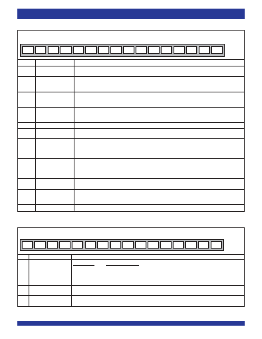
TABLE 5 — CONTROL REGISTER (CR) BITS
TABLE 6 — CONNECTION MEMORY BITS
Reset Value:
0000H
BIT
NAME
DESCRIPTION
15
SRS
A one will reset the device and have the same effect as the RESET pin. Must be zero for normal operation.
(SoftwareReset)
14
OEI
When1,theTX16-31/OutputEnableIndication0-15pinswillbeOutputEnableIndication0-15andreflect theactiveorhigh-impedance
(OutputEnableIndication)
state of their corresponding output data streams. When 0, this feature is disabled and these pins are used as output data streams
TX16-31.
13
OEPOL
When1,aoneonanOutputEnableIndicationpindenotesanactivestateontheoutputdatastream;zeroonanOutputEnableIndication
(Output Enable Polarity)
pin denotes high-impedance state. When 0, a one on an Output Enable Indication pin denotes high-impedance and a zero denotes
an active state.
12
AOE
When 1, TX0-31 will behave as Output Enable Indication0-31 accordingly. These outputs will reflect the active or high-impedance
(All Output Enable)
stateofthecorrespondingoutputdatastreams(TX0-31)inanotherIDT72V73260ifprogrammedidentically. When0,theTSIoperates
in the normal switch mode.
11-10
Unused
Must be zero for normal operation.
9
MBP
When 1, the Connection Memory block programming feature is ready for the programming of Connection Memory HIGH bits,
(Memory Block Program)
bit 14 to bit 15. When 0, this feature is disabled.
8-7
BPD1-0
These bits carry the value to be loaded into the Connection Memory block whenever the memory block programming feature
(Block Programming
is activated. After the Memory Block Program bit in the Control Register is set to 1 and the Block Programming Enable is set to 1,
Data)
the contents of the bits BPD1-0 are loaded into bit 15 and 14 of the Connection Memory. Bit 13 to bit 0 of the Connection Memory
are set to 0.
6
BPE
Azerotoonetransitionofthisbitenablesthememoryblockprogrammingfunction.TheBlockProgrammingEnableandBPD1-0bits
(Begin Block
in the Control Register have to be defined in the same write operation. Once the Block Programming Enable bit is set HIGH, the
ProgrammingEnable)
devicerequirestwoframestocompletetheblockprogramming.Aftertheprogrammingfunctionhasfinished,theBlockProgramming
Enable, Memory Block Program and BPD 1-0 bits will be reset to zero by the device to indicate the operation is complete.
5
OSB
When ODE = 0 and Output Stand By = 0, the output drivers of the transmit serial streams are in high-impedance mode. When
(Output Stand By)
either ODE =1 or Output Stand By =1, the output serial streams drivers function normally.
4
SFE
AzerotoonetransitioninthisbitstartstheFrameEvaluationprocedure.WhentheCompleteFrameEvaluationbitintheFrameAlignment
(Start Frame Evaluation)
Register changes from zero to one, the evaluation procedure stops. To start another Frame Evaluation cycle, set this bit to
zero for at least one frame.
3-0
Unused
Must be zero for normal operation.
15
14
13
12
11
10
9876543210
SRS
OEI
OEPOL
AOE
0
MBP
BPD1
BPD0
BPE
OSB
SFE
0000
15
14
13
12
11
10
9876543210
MOD1
MOD0
SAB4
SAB3
SAB2
SAB1
SAB0
CAB8
CAB7
CAB6
CAB5
CAB4
CAB3
CAB2
CAB1
CAB0
Bit
Name
Description
15, 14
MOD1-0
MOD1 MOD0
MODE
(Switching Mode Selection)
0
Variable Delay mode
0
1
Constant Delay mode
1
0
Processor mode
1
Outputhigh-impedance
13-9
SAB4-0
The binary value is the number of the data stream for the source of the connection.
(Source Stream Address Bits)
8-0
CAB8-0
The binary value is the number of the channel for the source of the connection.
(Source Channel Address Bits)
相关PDF资料 |
PDF描述 |
|---|---|
| M83723/76W22128 | CONN PLUG 12POS STRAIGHT W/PINS |
| VI-2VN-MX-B1 | CONVERTER MOD DC/DC 18.5V 75W |
| VI-2VL-MX-B1 | CONVERTER MOD DC/DC 28V 75W |
| VI-2VK-MX-B1 | CONVERTER MOD DC/DC 40V 75W |
| MAX5389LAUD+T | IC DGTL POT 256POS 10K 14TSSOP |
相关代理商/技术参数 |
参数描述 |
|---|---|
| IDT72V73260DAG | 功能描述:IC DGTL SW 16384X16384 144-TQFP RoHS:是 类别:集成电路 (IC) >> 逻辑 - 信号开关,多路复用器,解码器 系列:72V 标准包装:48 系列:74VHC 类型:多路复用器 电路:4 x 2:1 独立电路:1 输出电流高,低:8mA,8mA 电压电源:单电源 电源电压:2 V ~ 5.5 V 工作温度:-40°C ~ 85°C 安装类型:表面贴装 封装/外壳:16-SOIC(0.154",3.90mm 宽) 供应商设备封装:16-SOIC 包装:管件 |
| IDT72V73263BB | 功能描述:IC DGTL SW 16384X16384 208-BGA RoHS:否 类别:集成电路 (IC) >> 逻辑 - 信号开关,多路复用器,解码器 系列:72V 标准包装:48 系列:74VHC 类型:多路复用器 电路:4 x 2:1 独立电路:1 输出电流高,低:8mA,8mA 电压电源:单电源 电源电压:2 V ~ 5.5 V 工作温度:-40°C ~ 85°C 安装类型:表面贴装 封装/外壳:16-SOIC(0.154",3.90mm 宽) 供应商设备封装:16-SOIC 包装:管件 |
| IDT72V73273BB | 功能描述:IC DGTL SW 32768X32768 208-BGA RoHS:否 类别:集成电路 (IC) >> 逻辑 - 信号开关,多路复用器,解码器 系列:72V 标准包装:48 系列:74VHC 类型:多路复用器 电路:4 x 2:1 独立电路:1 输出电流高,低:8mA,8mA 电压电源:单电源 电源电压:2 V ~ 5.5 V 工作温度:-40°C ~ 85°C 安装类型:表面贴装 封装/外壳:16-SOIC(0.154",3.90mm 宽) 供应商设备封装:16-SOIC 包装:管件 |
| IDT72V73273BBG | 功能描述:IC DGTL SW 32768X32768 208-BGA RoHS:是 类别:集成电路 (IC) >> 逻辑 - 信号开关,多路复用器,解码器 系列:72V 标准包装:48 系列:74VHC 类型:多路复用器 电路:4 x 2:1 独立电路:1 输出电流高,低:8mA,8mA 电压电源:单电源 电源电压:2 V ~ 5.5 V 工作温度:-40°C ~ 85°C 安装类型:表面贴装 封装/外壳:16-SOIC(0.154",3.90mm 宽) 供应商设备封装:16-SOIC 包装:管件 |
| IDT72V801L10PF | 功能描述:IC SYNC FIFO 256X9 10NS 64QFP RoHS:否 类别:集成电路 (IC) >> 逻辑 - FIFO 系列:72V 标准包装:90 系列:7200 功能:同步 存储容量:288K(16K x 18) 数据速率:100MHz 访问时间:10ns 电源电压:4.5 V ~ 5.5 V 工作温度:0°C ~ 70°C 安装类型:表面贴装 封装/外壳:64-LQFP 供应商设备封装:64-TQFP(14x14) 包装:托盘 其它名称:72271LA10PF |
发布紧急采购,3分钟左右您将得到回复。