- 您现在的位置:买卖IC网 > PDF目录10043 > IDT72V801L15PFI8 (IDT, Integrated Device Technology Inc)IC SYNC FIFO 256X9 15NS 64QFP PDF资料下载
参数资料
| 型号: | IDT72V801L15PFI8 |
| 厂商: | IDT, Integrated Device Technology Inc |
| 文件页数: | 13/16页 |
| 文件大小: | 0K |
| 描述: | IC SYNC FIFO 256X9 15NS 64QFP |
| 标准包装: | 750 |
| 系列: | 72V |
| 功能: | 异步 |
| 存储容量: | 2.3K(256 x 9) |
| 数据速率: | 67MHz |
| 访问时间: | 15ns |
| 电源电压: | 3 V ~ 3.6 V |
| 工作温度: | -40°C ~ 85°C |
| 安装类型: | 表面贴装 |
| 封装/外壳: | 64-LQFP |
| 供应商设备封装: | 64-TQFP(14x14) |
| 包装: | 带卷 (TR) |
| 其它名称: | 72V801L15PFI8 |
6
IDT72V801/72V8211/72V821/72V831/72V841/72V851 3.3V DUAL CMOS SyncFIFOTM
DUAL 256 x 9, DUAL 512 x 9, DUAL 1K x 9, DUAL 2K x 9, DUAL 4K x 9, DUAL 8K x 9
COMMERCIAL AND INDUSTRIAL
TEMPERATURE RANGES
OCTOBER 22, 2008
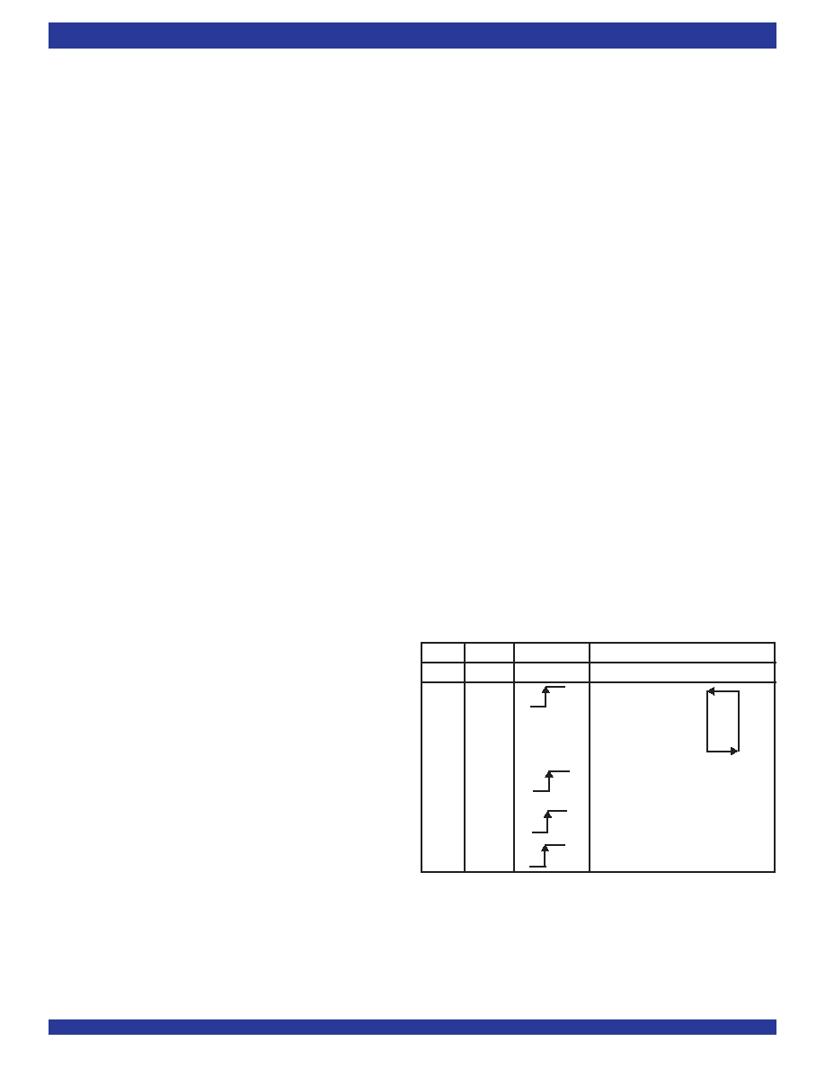
LDA
WENA1
WCLKA
OPERATION ON FIFO A
LDB
WENB1
WCLKB
OPERATION ON FIFO B
0
Empty Offset (LSB)
Empty Offset (MSB)
Full Offset (LSB)
Full Offset (MSB)
0
1
No Operation
1
0
Write Into FIFO
1
No Operation
Figure 2. Writing to Offset Registers for FIFOs A and B
When either of the two Read Enable,
RENA1, RENA2 (RENB1, RENB2)
associated with FIFO A (B) is HIGH, the output register holds the previous data
and no new data is allowed to be loaded into the register.
When all the data has been read from FIFO A (B), the Empty Flag,
EFA
(
EFB) will go LOW, inhibiting further read operations. Once a valid write
operation has been accomplished,
EFA (EFB) will go HIGH after tREF and a
valid read can begin. The Read Enables,
RENA1, RENA2(RENB1, RENB2)
are ignored when FIFO A (B) is empty.
Output Enable (
OEA, OEB) — When Output Enable, OEA (OEB) is
enabled(LOW),theparalleloutputbuffersofFIFOA(B)receivedatafromtheir
respective output register. When Output Enable,
OEA (OEB) is disabled
(HIGH), the QA (QB) output data bus is in a high-impedance state.
Write Enable 2/Load (WENA2/
LDA, WENB2/LDB) — This is a dual-
purpose pin. FIFO A (B) is configured at Reset to have programmable flags
or to have two write enables, which allows depth expansion. If WENA2/
LDA
(WENB2/
LDB) issetHIGHatReset,RSA=LOW(RSB=LOW),thispinoperates
as a second Write Enable pin.
If FIFO A (B) is configured to have two write enables, when Write Enable
1,
WENA1(WENB1)isLOWandWENA2/LDA(WENB2/LDB)isHIGH,datacan
beloadedintotheinputregisterandRAMarrayontheLOW-to-HIGHtransition
ofeveryWriteClock,WCLKA(WCLKB). Dataisstoredinthearraysequentially
and independently of any on-going read operation.
In this configuration, when
WENA1(WENB1)isHIGHand/orWENA2/LDA
(WENB2/
LDB) is LOW, the input register of Array A holds the previous data
and no new data is allowed to be loaded into the register.
To prevent data overflow, the Full Flag,
FFA(FFB) will go LOW, inhibiting
further write operations. Upon the completion of a valid read cycle,
FFA(FFB)
will go HIGH after tWFF, allowing a valid write to begin.
WENA1, (WENB1) and
WENA2/
LDA(WENB2/LDB) are ignored when the FIFO is full.
FIFO A (B) is configured to have programmable flags when the WENA2/
LDA(WENB2/LDB)issetLOWatReset,RSA = LOW(RSB = LOW). EachFIFO
SIGNAL DESCRIPTIONS
FIFO A and FIFO B are identical in every respect. The following description
explainstheinteractionofinputandoutputsignalsforFIFOA.Thecorrespond-
ing signal names for FIFO B are provided in parentheses.
INPUTS:
Data In (DA0 – DA8, DB0 – DB8) — DA0 - DA8 are the nine data inputs
for memory array A. DB0 - DB8 are the nine data inputs for memory array B.
CONTROLS:
Reset (
RSA,RSB)—ResetofFIFOA(B)isaccomplishedwheneverRSA
(
RSB) input is taken to a LOW state. During reset, the internal read and write
pointersassociatedwiththeFIFOaresettothefirstlocation.Aresetisrequired
after power-up before a write operation can take place. The Full Flag,
FFA
(
FFB)andProgrammableAlmost-FullFlag,PAFA(PAFB)willberesettoHIGH
aftertRSF. TheEmptyFlag,
EFA(EFB)andProgrammableAlmost-EmptyFlag,
PAEA(PAEB)willberesettoLOWaftertRSF. Duringreset,theoutputregister
is initialized to all zeros and the offset registers are initialized to their default
values.
Write Clock (WCLKA, WCLKB) — A write cycle to Array A (B) is initiated
on the LOW-to-HIGH transition of WCLKA (WCLKB). Data set-up and hold
times must be met with respect to the LOW-to-HIGH transition of WCLKA
(WCLKB). The Full Flag,
FFA (FFB) and Programmable Almost-Full Flag,
PAFA(PAFB)aresynchronizedwithrespecttotheLOW-to-HIGHtransitionof
the Write Clock, WCLKA (WCLKB).
The Write and Read clock can be asynchronous or coincident.
Write Enable 1 (
WENA1, WENB1) — If FIFO A (B) is configured for
programmable flags,
WENA1(WENB1) is the only enable control pin. In this
configuration,when
WENA1(WENB1)isLOW,datacanbeloadedintotheinput
register of RAM Array A (B) on the LOW-to-HIGH transition of every Write
Clock, WCLKA (WCLKB). Data is stored in Array A (B) sequentially and
independently of any on-going read operation.
In this configuration, when
WENA1 (WENB1) is HIGH, the input register
holds the previous data and no new data is allowed to be loaded into the
register.
If the FIFO is configured to have two write enables, which allows for depth
expansion. See Write Enable 2 paragraph below for operation in this
configuration.
To prevent data overflow,
FFA(FFB) will go LOW, inhibiting further write
operations. Upon the completion of a valid read cycle, the
FFA(FFB) will go
HIGH after tWFF, allowing a valid write to begin.
WENA1(WENB1) is ignored
when FIFO A (B) is full.
Read Clock (RCLKA, RCLKB) — Data can be read from Array A (B)
on the LOW-to-HIGH transition of RCLKA (RCLKB). The Empty Flag,
EFA
(
EFB)andProgrammableAlmost-EmptyFlag,PAEA(PAEB)aresynchronized
with respect to the LOW-to-HIGH transition of RCLKA (RCLKB).
The Write and Read Clock can be asynchronous or coincident.
Read Enables (
RENA1, RENA2, RENB1, RENB2) — When both Read
Enables,
RENA1, RENA2(RENB1, RENB2) are LOW, data is read from Array
A (B) to the output register on the LOW-to-HIGH transition of the Read Clock,
RCLKA (RCLKB).
NOTE:
4093 tbl 08
1. For the purposes of this table, WENA2 and WENB2 = VIH.
2. The same selection sequence applies to reading from the registers.
RENA1 and RENA2
(
RENB1 and RENB2) are enabled and read is performed on the LOW-to-HIGH transition
of RCLKA (RCLKB).
相关PDF资料 |
PDF描述 |
|---|---|
| LTC1350ISW | IC TXRX 3.3V EIA/TIA-562 28-SOIC |
| VE-B6F-MW-F4 | CONVERTER MOD DC/DC 72V 100W |
| MS3106R28-11SX | CONN PLUG 22POS STRAIGHT W/SCKT |
| VI-B1Z-MX | CONVERTER MOD DC/DC 2V 30W |
| VI-BN1-IV-F4 | CONVERTER MOD DC/DC 12V 150W |
相关代理商/技术参数 |
参数描述 |
|---|---|
| IDT72V801L15TF | 功能描述:IC SYNC FIFO 256X9 15NS 64QFP RoHS:否 类别:集成电路 (IC) >> 逻辑 - FIFO 系列:72V 标准包装:90 系列:7200 功能:同步 存储容量:288K(16K x 18) 数据速率:100MHz 访问时间:10ns 电源电压:4.5 V ~ 5.5 V 工作温度:0°C ~ 70°C 安装类型:表面贴装 封装/外壳:64-LQFP 供应商设备封装:64-TQFP(14x14) 包装:托盘 其它名称:72271LA10PF |
| IDT72V801L15TF8 | 功能描述:IC SYNC FIFO 256X9 15NS 64QFP RoHS:否 类别:集成电路 (IC) >> 逻辑 - FIFO 系列:72V 标准包装:80 系列:7200 功能:同步 存储容量:18.4K(1K x 18) 数据速率:- 访问时间:10ns 电源电压:4.5 V ~ 5.5 V 工作温度:0°C ~ 70°C 安装类型:表面贴装 封装/外壳:64-LQFP 供应商设备封装:64-TQFP(10x10) 包装:托盘 其它名称:72225LB10TF |
| IDT72V801L15TFI | 功能描述:IC SYNC FIFO 256X9 15NS 64QFP RoHS:否 类别:集成电路 (IC) >> 逻辑 - FIFO 系列:72V 标准包装:90 系列:7200 功能:同步 存储容量:288K(16K x 18) 数据速率:100MHz 访问时间:10ns 电源电压:4.5 V ~ 5.5 V 工作温度:0°C ~ 70°C 安装类型:表面贴装 封装/外壳:64-LQFP 供应商设备封装:64-TQFP(14x14) 包装:托盘 其它名称:72271LA10PF |
| IDT72V801L15TFI8 | 功能描述:IC SYNC FIFO 256X9 15NS 64QFP RoHS:否 类别:集成电路 (IC) >> 逻辑 - FIFO 系列:72V 标准包装:90 系列:7200 功能:同步 存储容量:288K(16K x 18) 数据速率:100MHz 访问时间:10ns 电源电压:4.5 V ~ 5.5 V 工作温度:0°C ~ 70°C 安装类型:表面贴装 封装/外壳:64-LQFP 供应商设备封装:64-TQFP(14x14) 包装:托盘 其它名称:72271LA10PF |
| IDT72V801L20PF | 功能描述:IC SYNC FIFO 256X9 20NS 64QFP RoHS:否 类别:集成电路 (IC) >> 逻辑 - FIFO 系列:72V 标准包装:90 系列:7200 功能:同步 存储容量:288K(16K x 18) 数据速率:100MHz 访问时间:10ns 电源电压:4.5 V ~ 5.5 V 工作温度:0°C ~ 70°C 安装类型:表面贴装 封装/外壳:64-LQFP 供应商设备封装:64-TQFP(14x14) 包装:托盘 其它名称:72271LA10PF |
发布紧急采购,3分钟左右您将得到回复。