- 您现在的位置:买卖IC网 > PDF目录10093 > IDT72V82L20PA (IDT, Integrated Device Technology Inc)IC FIFO ASYNCH 1KX9 56TSSOP PDF资料下载
参数资料
| 型号: | IDT72V82L20PA |
| 厂商: | IDT, Integrated Device Technology Inc |
| 文件页数: | 1/12页 |
| 文件大小: | 0K |
| 描述: | IC FIFO ASYNCH 1KX9 56TSSOP |
| 标准包装: | 34 |
| 系列: | 72V |
| 功能: | 异步 |
| 存储容量: | 9K(1K x 9) |
| 数据速率: | 33MHz |
| 访问时间: | 20ns |
| 电源电压: | 3 V ~ 3.6 V |
| 工作温度: | 0°C ~ 70°C |
| 安装类型: | 表面贴装 |
| 封装/外壳: | 56-TFSOP(0.240",6.10mm 宽) |
| 供应商设备封装: | 56-TSSOP |
| 包装: | 管件 |
| 其它名称: | 72V82L20PA |
1
DSC-3966/5
JUNE 2012
IDT72V81
IDT72V82
IDT72V83
IDT72V84
IDT72V85
3.3 Volt CMOS DUAL ASYNCHRONOUS FIFO
DUAL 512 x 9, DUAL 1,024 x 9
DUAL 2,048 x 9, DUAL 4,096 X 9
DUAL 8,192 X 9
2012 Integrated Device Technology, Inc. All rights reserved. Product specifications subject to change without notice.
IDT and the IDT logo are registered trademarks of Integrated Device Technology, Inc. The AsyncFIFO
isatrademarkofIntegratedDeviceTechnology,Inc.
COMMERCIAL AND INDUSTRIAL TEMPERATURE RANGES
FEATURES:
The IDT72V81 is equivalent to two IDT72V01 - 512 x 9 FIFOs
The IDT72V82 is equivalent to two IDT72V02 - 1,024 x 9 FIFOs
The IDT72V83 is equivalent to two IDT72V03 - 2,048 x 9 FIFOs
The IDT72V84 is equivalent to two IDT72V04 - 4,096 x 9 FIFOs
The IDT72V85 is equivalent to two IDT72V05 - 8,192 x 9 FIFOs
Low power consumption
— Active: 330 mW (max.)
— Power-down: 18 mW (max.)
Ultra high speed—15 ns access time
Asynchronous and simultaneous read and write
Offers optimal combination of data capacity, small foot print
and functional flexibility
Ideal for bidirectional, width expansion, depth expansion, bus-
matching, and data sorting applications
Status Flags: Empty, Half-Full, Full
Auto-retransmit capability
High-performance CMOS technology
Space-saving TSSOP package
Industrial temperature range (–40
°°°°°C to +85°°°°°C) is available
Green parts available, see ordering information
DESCRIPTION:
TheIDT72V81/72V82/72V83/72V84/72V85aredual-FIFOmemoriesthat
loadandemptydataonafirst-in/first-outbasis.Thesedevicesarefunctionaland
compatible to two IDT72V01/72V02/72V03/72V04/72V05 FIFOs in a single
packagewithallassociatedcontrol,data,andflaglinesassignedtoseparate
pins. The devices use Full and Empty flags to prevent data overflow and
underflowandexpansionlogictoallowforunlimitedexpansioncapabilityinboth
word size and depth.
The reads and writes are internally sequential through the use of ring
pointers,withnoaddressinformationrequiredtoloadandunloaddata. Data
istoggledinandoutofthedevicesthroughtheuseoftheWrite(W)andRead
(R) pins.
The devices utilize a 9-bit wide data array to allow for control and parity
bitsattheuser’soption.Thisfeatureis especiallyusefulindatacommunications
applicationswhereitisnecessarytouseaparitybitfortransmission/reception
errorchecking.ItalsofeaturesaRetransmit(RT)capabilitythatallowsforreset
of the read pointer to its initial position when RT is pulsed low to allow for
retransmission from the beginning of data. A Half-Full Flag is available in the
single device mode and width expansion modes.
TheseFIFOsarefabricatedusinghigh-speedCMOStechnology.Theyare
designed for those applications requiring asynchronous and simultaneous
read/writesinmultiprocessingandratebufferapplications.
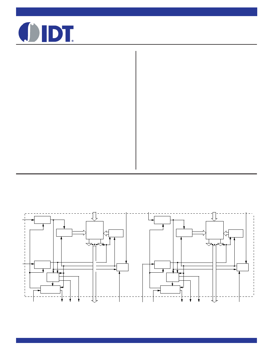
FUNCTIONAL BLOCK DIAGRAM
WA
WRITE
CONTROL
READ
CONTROL
RA
FLAG
LOGIC
EXPANSION
LOGIC
XIA
WRITE
POINTER
RAM
ARRAY A
512 x 9
1,024 x 9
2,048 x 9
4,096 x 9
8,192 x 9
READ
POINTER
DATA INPUTS
RESET
LOGIC
THREE-
STATE
BUFFERS
DATA
OUTPUTS
RSA
FLA/RTA
XOA/HFA
FFA
EFA
WB
WRITE
CONTROL
READ
CONTROL
RB
FLAG
LOGIC
EXPANSION
LOGIC
XIB
WRITE
POINTER
READ
POINTER
DATA INPUTS
RESET
LOGIC
THREE-
STATE
BUFFERS
DATA
OUTPUTS
RSB
FLB/RTB
3966 drw 01
XOB/HFB
FFB
EFB
(DA0-DA8)
(QA0-QA8)
(QB0-QB8)
(DB0-DB8)
RAM
ARRAY A
512 x 9
1,024 x 9
2,048 x 9
4,096 x 9
8,192 x 9
相关PDF资料 |
PDF描述 |
|---|---|
| GTC06AF-14S-6S | CONN PLUG 6POS STRAIGHT W/SCKT |
| VE-2ND-MX-F2 | CONVERTER MOD DC/DC 85V 75W |
| MS3101A22-4P | CONN RCPT 4POS FREE HNG W/PINS |
| MS27505E17F35SC | CONN RCPT 55POS BOX MNT W/SCKT |
| VI-2TT-MY | CONVERTER MOD DC/DC 6.5V 50W |
相关代理商/技术参数 |
参数描述 |
|---|---|
| IDT72V82L20PA8 | 功能描述:IC FIFO ASYNCH 1KX9 56TSSOP RoHS:否 类别:集成电路 (IC) >> 逻辑 - FIFO 系列:72V 标准包装:80 系列:7200 功能:同步 存储容量:18.4K(1K x 18) 数据速率:- 访问时间:10ns 电源电压:4.5 V ~ 5.5 V 工作温度:0°C ~ 70°C 安装类型:表面贴装 封装/外壳:64-LQFP 供应商设备封装:64-TQFP(10x10) 包装:托盘 其它名称:72225LB10TF |
| IDT72V82L20PAI | 制造商:Integrated Device Technology Inc 功能描述:IC FIFO ASYNCH 1KX9 56TSSOP |
| IDT72V82L20PAI8 | 制造商:Integrated Device Technology Inc 功能描述:IC FIFO ASYNCH 1KX9 56TSSOP |
| IDT72V831L10PF | 功能描述:IC SYNC FIFO 2048X9 10NS 64QFP RoHS:否 类别:集成电路 (IC) >> 逻辑 - FIFO 系列:72V 标准包装:90 系列:7200 功能:同步 存储容量:288K(16K x 18) 数据速率:100MHz 访问时间:10ns 电源电压:4.5 V ~ 5.5 V 工作温度:0°C ~ 70°C 安装类型:表面贴装 封装/外壳:64-LQFP 供应商设备封装:64-TQFP(14x14) 包装:托盘 其它名称:72271LA10PF |
| IDT72V831L10PF8 | 功能描述:IC SYNC FIFO 2048X9 10NS 64QFP RoHS:否 类别:集成电路 (IC) >> 逻辑 - FIFO 系列:72V 标准包装:90 系列:7200 功能:同步 存储容量:288K(16K x 18) 数据速率:100MHz 访问时间:10ns 电源电压:4.5 V ~ 5.5 V 工作温度:0°C ~ 70°C 安装类型:表面贴装 封装/外壳:64-LQFP 供应商设备封装:64-TQFP(14x14) 包装:托盘 其它名称:72271LA10PF |
发布紧急采购,3分钟左右您将得到回复。